AD7294 Просмотр технического описания (PDF) - Analog Devices
Номер в каталоге
Компоненты Описание
производитель
AD7294 Datasheet PDF : 45 Pages
| |||
AD7294
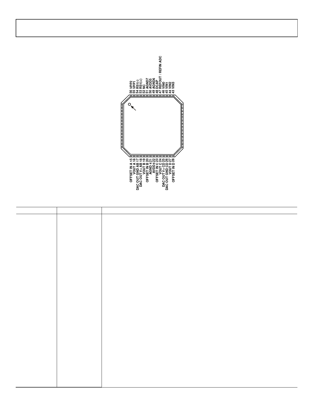
PIN CONFIGURATION AND FUNCTION DESCRIPTIONS
Preliminary Technical Data
RS2 (-) 1
RS2(+) 2
NC 3
AVDD1 4
AGND1 5
AGND2 6
AVDD2 7
D2(-) 8
D2(+) 9
D1(+) 10
D1(-) 11
AGND3 12
AVDD3 13
REFOUT / REFIN DAC 14
NC = NO CONNECT
PIN 1
INDICATOR
AD7294
TOP VIEW
(Not to scale)
42 NC
41 ISENSE 1 OVERRANGE
40 ISENSE 2 OVERRANGE
39 DVDD
38 DGND
37 VDRIVE
36 OPGND
35 SCL
34 SDA (I2C) / SDI (SPI)
33 AS0 (I2C) / SDO (SPI)
32 AS1 (I2C) / CSB (SPI)
31 AS2 (I2C) / ALERT (SPI)
30 ALERT (I2C) / AGND6 (SPI)
29 AGND5
Table 4. Pin Function Descriptions
Pin No.
Mnemonic
1, 54
RS2(−), RS1(−)
2, 53
RS2(+), RS1(+)
3, 42, 52
NC
4, 7, 13, 22, 50
AVDD1 to AVDD5
5, 6, 12, 21,
29, 49, 51
8, 11
9, 10
14
AGND 1 to AGND7
D2(−), D1(−)
D2(+), D1(+)
REFOUT/REFIN DAC
15, 20, 23, 28
16, 19, 24, 27
OFFSET IN A to
OFFSET IN D
VOUT A to VOUT D
17, 18
25, 26
30
31 to 33
34
35
DAC OUT GND AB,
DAC OUT V+ AB
DAC OUT V+ CD,
DAC OUT GND CD
ALERT
AS2, AS1, AS0
SDA
SCL
Figure 4.
Description
Low-Side Connection for External Sense Resistor.
High-Side Connection for External Sense Resistor.
No Connection
Analog Supply Pins. These pins should be decoupled with a 0.1 µF ceramic capacitor and a 10 µF
tantalum capacitor. Operating range is 4.5 V to 5.5 V.
Analog Ground Reference Point. All AGND pins should be connected externally to the AGND
plane.
Analog Input. Connected to cathodes of the external temperature-sensing diodes.
Analog Input. Connected to anodes of the external temperature-sensing diodes.
The AD7294 contains a REFOUT/REFIN DAC pin common to all four DAC channels. When the
internal reference is selected, this pin is the reference output. If the application requires an
external reference, it can be applied to this pin, and the internal reference can be disabled via
the control register. The default for this pin is a reference input.
Used to set the desired output range for each DAC channel. Input range is 0 V to 5 V.
Buffered Analog Outputs for DAC Channels A to D. Each analog output is driven by an output
amplifier that can be offset using the offset in pin. DACs provide 12-bit resolution in a 5 V range,
providing an output voltage from 0 V to 15 V. Each output is capable of sourcing and sinking
10 mA and driving a 1,000 pF load.
Analog Supply Pins for Output Amplifiers on VOUTA and VOUTB.
Analog Supply Pins for Output Amplifiers on VOUTC and VOUTD.
Digital Output. This pin acts as an out-of-range indicator and becomes active when a conversion
result violates the DATAHIGH or DATALOW register values associated with each channel input.
Logic Inputs. These inputs are used to select unique addresses for the AD7294. Device address
depends on the voltage applied to these pins.
Digital I/O. Serial bus bidirectional data. Open-drain output.
Digital Input. Serial bus clock. The data transfer rate in I2C mode is compatible with both 100 kHz
Rev. PrB | Page 8 of 45
Share Link: 