AD7294 Просмотр технического описания (PDF) - Analog Devices
Номер в каталоге
Компоненты Описание
производитель
AD7294 Datasheet PDF : 45 Pages
| |||
Preliminary Technical Data
AD7294
SYSTEM DESCRIPTION
R Sense
VPP(1-2)
RS1(+) RS1(-)
RS2(+) RS2(-)
REFOUT/
REFOUT/
REFIN ADC REFIN DAC AVDD(1-5) AGND(1-9) V+(1-2)
RF CHOKE
FAULT2
FAULT1
VIN 0
VIN 1
VIN 2
VIN 3
D1 (+)
HIGH SIDE
CURRENT
SENSE
SET-POINT
240mV
HIGH SIDE
CURRENT
SENSE
MUX
2.5V
REF
12-BIT
ADC
12-BIT
DAC
100K
100K 200K
200K
12-BIT
DAC
100K
100K 200K
200K
VOUT A
FILTER
OFFSET IN A
VOUT B
FILTER
RF OUT
LDMOS
LDMOS
D0 (+)
T1
T0
D0 (-)
D1 (-)
AD7294
LIMIT
REGISTERS
TEMP
SENSOR
CONTROL
LOGIC
I2C INTERFACE
PROTOCOL
12-BIT
DAC
100K
100K 200K
200K
12-BIT
DAC
100K
100K 200K
200K
OFFSET IN B
VOUT C GAIN
CONTROL
OFFSET IN C
VOUT D
IMPEDANCE
MATCH
OFFSET IN D
DVDD DGND(1-2) SDA SCL A2 A1 A0 CAP ALERT
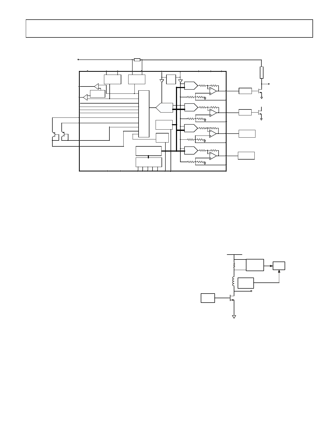
Figure 5. System Diagram
The AD7294 contains all the functions required for general-
purpose monitoring and control of current, voltage, and
temperature integrated into a single-chip solution. The part
includes low voltage (±200 mV) analog-input sense amplifiers
for current monitoring across shunt resistors, temperature-
sense inputs, and four uncommitted analog input channels
multiplexed into a 200 kSPS SAR ADC. Four 12-bit DACs
provide the outputs for voltage control and complete the
analog-to-digital digital-to-analog control loop. The DACs
provide digital control with 1.2 mV resolution to control the
bias currents of the power transistors; they can also be used to
provide control voltages for variable gain amplifiers or
impedance-match networks in the main signal chain.
The ADC monitors the high-side current and temperature
sensors as shown in Figure 6. If the temperature of, for
example, an LDMOS High Power Amplifier (HPA) transistor
rises above predetermined limits, out of limit comparisons
generate flags. The on-chip DAC will use the digital correction
loop to decrease the VGS of the device to maintain the desired
output voltage. An external resistor is used to sense the
transistors drain current and so automatically control the gate
bias voltage of the device.
VDD
RSENSE
CURRENT
SENSE
ADC
An internal, 2.5 V, low ppm reference is provided to drive both
the DAC and ADC. This internal reference can be overdriven
when an external reference is required. The AD7294 also
includes limit registers for alarm functions. Using alert registers,
the AD7294 flags an alert signal when the ADC readings go
above or below predetermined values. The analog input range
for the ADC can be selected to be a 0 V to VREF or 0 V to a
2×VREF input, configured with either single-ended or
differential analog inputs.
To compensate for temperature effects, one local on-chip, band
gap, temperature sensor and two remote, diode based,
temperature sensors can alternatively be selected. The high side
current sense is specified to manage LDMOS FETs up to 48 V
with bias currents ranging from 300 mA to 800 mA and gate
voltages of 4 V to 9 V. The part is designed on a high voltage
DMOS process for high voltage compliance, 60 V on the
current-sense inputs, and up to 15 V DAC output voltage.
RF CHOKE
DAC
VDRIVE
TEMP
SENSE
VOUTPUT
HPA
Figure 6. Simplified Diagram of System
The part is ideal for bias current control of the power transistors
in power amplifiers employed in CDMA, GSM, EDGE, and UMTS
cellular base stations. The I2C digital interface allows the
flexibility of programming the bias points using an external
controller. The I2C bus also allows a number of devices to be
connected in parallel to control multiple FETS, the standard in
single-carrier and multi-carrier base station systems.
Rev. PrB | Page 11 of 45
Share Link: 