AD7225 Просмотр технического описания (PDF) - Analog Devices
Номер в каталоге
Компоненты Описание
производитель
AD7225 Datasheet PDF : 24 Pages
| |||
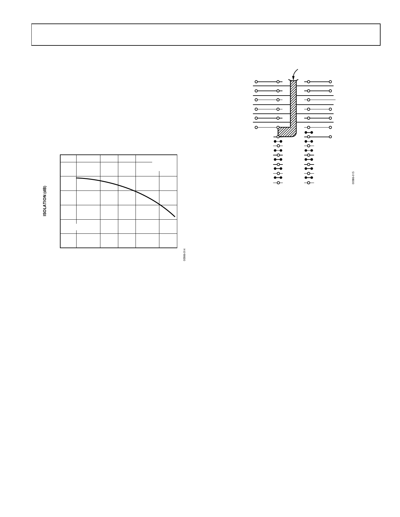
GROUND MANAGEMENT AND LAYOUT
Because the AD7225 contains four reference inputs that can be
driven from ac sources (see the AC Reference Signal section),
careful layout and grounding is important to minimize analog
crosstalk between the four channels. The dynamic performance
of the four DACs depends on the optimum choice of board
layout. Figure 14 shows the relationship between input fre-
quency and channel-to-channel isolation. Figure 15 shows a
printed circuit board layout that minimizes crosstalk and
feedthrough. The four input signals are screened by AGND.
VREF was limited to between 2 V and 3.24 V to avoid slew rate
limiting effects from the output amplifier during measurements.
VDD = +15V
–80
VSS = –5V
TA = 25°C
–70
–60
–50
–40
VREF = 1.24V p-p
–30
20k
50k
100k 200k
500k
1M
INPUT FREQUENCY (Hz)
Figure 14. Channel-to-Channel Isolation
AD7225
VOUTB
VOUTA
VSS
VREFB
VREFA
AGND
DGND
PIN 1
MSB
SYSTEM
GND
VOUTC
VOUTD
VDD
VREFC
VREFD
LSB
Figure 15. Suggested PCB Layout for AD7225, Component Side (Top View)
Rev. C | Page 11 of 24
Share Link: 