AD7225CQ Просмотр технического описания (PDF) - Analog Devices
Номер в каталоге
Компоненты Описание
производитель
AD7225CQ Datasheet PDF : 12 Pages
| |||
AD7225
ABSOLUTE MAXIMUM RATINGS1
VDD to AGND . . . . . . . . . . . . . . . . . . . . . . . . . . –0.3 V, +17 V
VDD to DGND . . . . . . . . . . . . . . . . . . . . . . . . . . –0.3 V, +17 V
VDD to VSS . . . . . . . . . . . . . . . . . . . . . . . . . . . . . –0.3 V, +24 V
AGND to DGND . . . . . . . . . . . . . . . . . . . . . . . . –0.3 V, VDD
Digital Input Voltage to DGND . . . . . . . –0.3 V, VDD + 0.3 V
VREF to AGND . . . . . . . . . . . . . . . . . . . . –0.3 V, VDD + 0.3 V
VOUT to AGND2 . . . . . . . . . . . . . . . . . . . . . . . . . . . . VSS, VDD
Power Dissipation (Any Package) to +75°C . . . . . . . . 500 mW
Derates above 75°C by . . . . . . . . . . . . . . . . . . . . . 2.0 mW/°C
Operating Temperature
Commercial (K, L Versions) . . . . . . . . . . . –40°C to +85°C
Industrial (B, C Versions) . . . . . . . . . . . . . –40°C to +85°C
Extended (T, U Versions) . . . . . . . . . . . . –55°C to +125°C
Storage Temperature . . . . . . . . . . . . . . . . . . –65°C to +150°C
Lead Temperature (Soldering, 10 secs) . . . . . . . . . . . +300°C
NOTES
1Stresses above those listed under “Absolute Maximum Ratings” may cause
permanent damage to the device. This is a stress rating only and functional
operation of the device at these or any other conditions above those indicated in
the operational sections of this specification is not implied. Exposure to absolute
maximum rating conditions for extended periods may affect device reliability.
2Outputs may be shorted to any voltage in the range VSS to VDD provided that the
power dissipation of the package is not exceeded. Typical short circuit current for
a short to AGND or VSS is 50 mA.
CAUTION
ESD (electrostatic discharge) sensitive device. Electrostatic charges as high as 4000 V readily
accumulate on the human body and test equipment and can discharge without detection.
Although the AD7225 features proprietary ESD protection circuitry, permanent damage may
occur on devices subjected to high energy electrostatic discharges. Therefore, proper ESD
precautions are recommended to avoid performance degradation or loss of functionality.
WARNING!
ESD SENSITIVE DEVICE
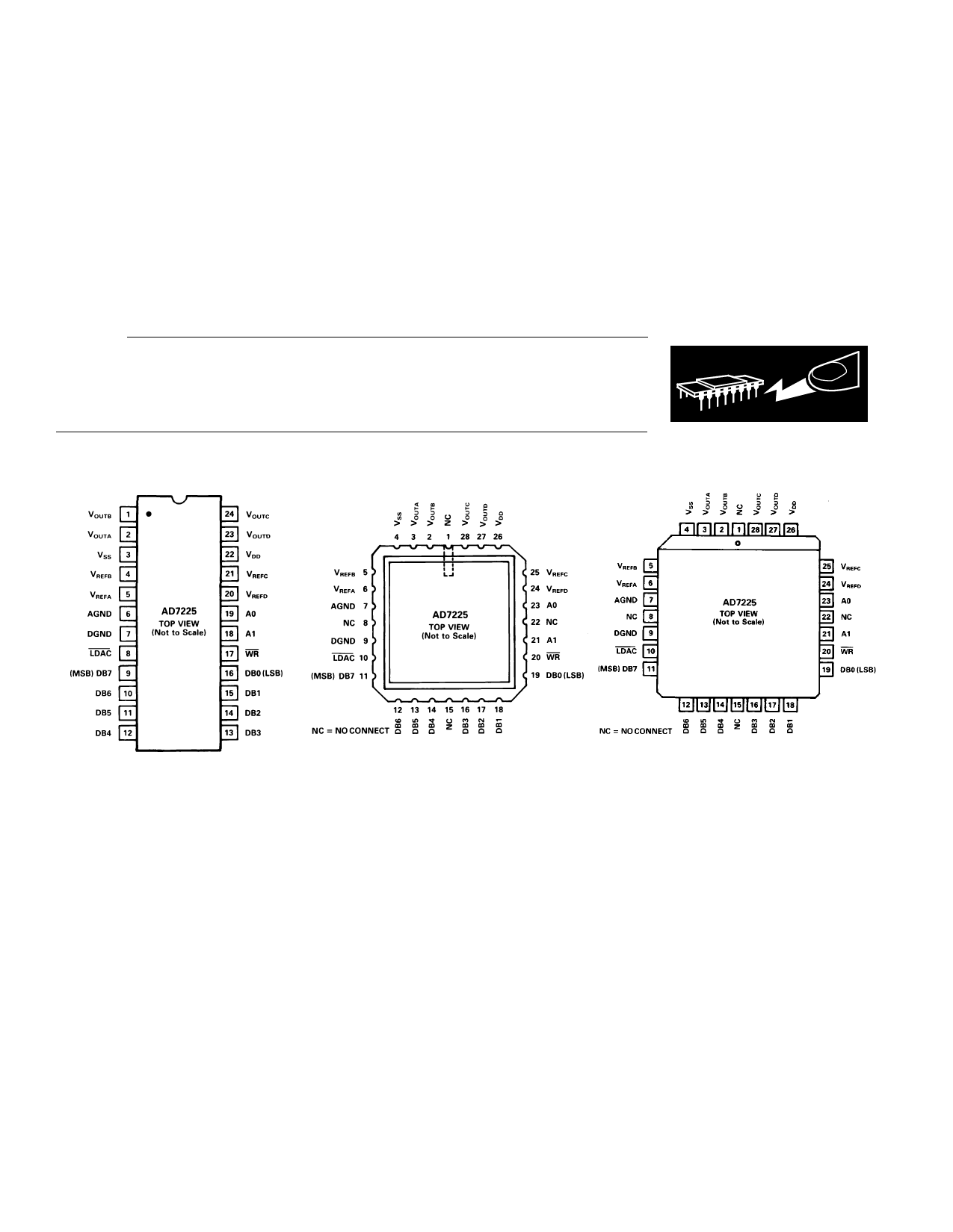
DIP and SOIC
PIN CONFIGURATIONS
LCCC
PLCC
TERMINOLOGY
TOTAL UNADJUSTED ERROR
Total Unadjusted Error is a comprehensive specification which
includes full-scale error, relative accuracy, and zero code error.
Maximum output voltage is VREF – 1 LSB (ideal), where 1 LSB
(ideal) is VREF/256. The LSB size will vary over the VREF range.
Hence the zero code error will, relative to the LSB size, increase
as VREF decreases. Accordingly, the total unadjusted error,
which includes the zero code error, will also vary in terms of
LSBs over the VREF range. As a result, total unadjusted error is
specified for a fixed reference voltage of +10 V.
RELATIVE ACCURACY
Relative Accuracy or endpoint nonlinearity is a measure of the
maximum deviation from a straight line passing through the
endpoints of the DAC transfer function. It is measured after al-
lowing for zero code error and full-scale error and is normally
expressed in LSBs or as a percentage of full-scale reading.
DIFFERENTIAL NONLINEARITY
Differential Nonlinearity is the difference between the measured
change and the ideal 1 LSB change between any two adjacent
codes. A specified differential nonlinearity of ± 1 LSB max over
the operating temperature range ensures monotonicity.
DIGITAL FEEDTHROUGH
Digital Feedthrough is the glitch impulse transferred to the out-
put of the DAC due to a change in its digital input code. It is
specified in nV secs and is measured at VREF = 0 V.
DIGITAL CROSSTALK
Digital Crosstalk is the glitch impulse transferred to the output
of one converter (not addressed) due to a change in the digital
input code to another addressed converter. It is specified in
nV secs and is measured at VREF = 0 V.
AC FEEDTHROUGH
AC Feedthrough is the proportion of reference input signal
which appears at the output of a converter when that DAC is
loaded with all 0s.
CHANNEL-TO-CHANNEL ISOLATION
Channel-to-channel isolation is the proportion of input signal
from the reference of one DAC (loaded with all 1s) which ap-
pears at the output of one of the other three DACs (loaded with
all 0s) The figure given is the worst case for the three other out-
puts and is expressed as a ratio in dBs.
FULL-SCALE ERROR
Full-Scale Error is defined as:
Measured Value – Zero Code Error – Ideal Value
–4–
REV. B
Share Link: 