AD6122ACPRL Просмотр технического описания (PDF) - Analog Devices
Номер в каталоге
Компоненты Описание
производитель
AD6122ACPRL Datasheet PDF : 20 Pages
| |||
AD6122
VCC
I INPUT
LOCAL
OSCILLATOR
INPUT
Q INPUT
COMMON-MODE
REFERENCE
OUTPUT
VPOS
QUADRATURE
MODULATOR
OUTPUT
QUADRATURE MODULATOR
ATTENUATOR
،2
LOW
DROPOUT
REGULATOR
VREG
AD6122
GAIN
CONTROL
SCALE
FACTOR
IF AMPLIFIER
INPUT
IF AMPLIFIERS
TRANSMIT
OUTPUT
TEMPERATURE
COMPENSATION
POWER- POWER-
DOWN 1 DOWN 2
1.23 V
REFERENCE
OUTPUT
GAIN CONTROL
REFERENCE
VOLTAGE
INPUT
GAIN CONTROL
VOLTAGE
INPUT
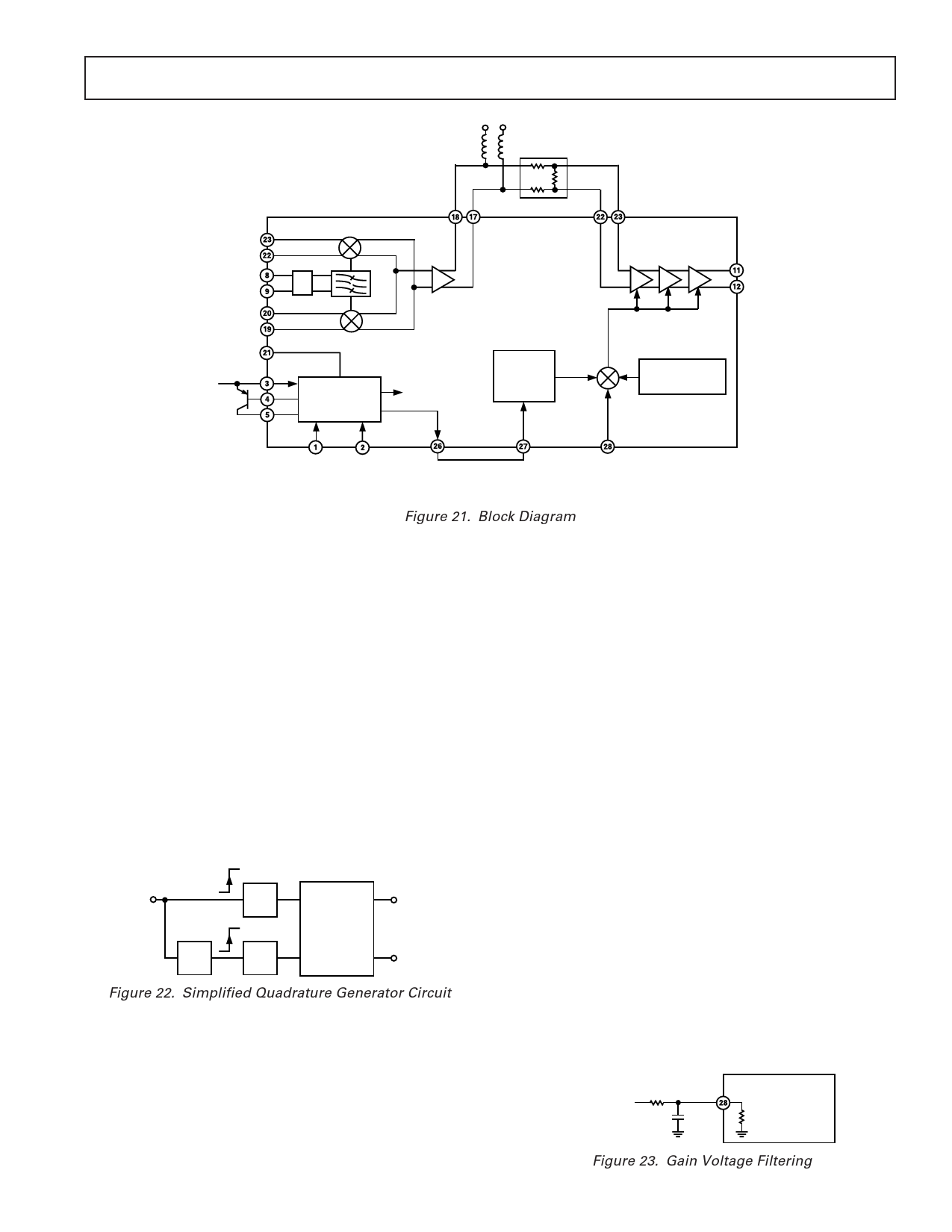
Figure 21. Block Diagram
THEORY OF OPERATION
The CDMA Transmitter IF Subsystem (Figure 21) consists of
an I and Q modulator with a divide-by-two quadrature genera-
tor, high dynamic range IF amplifiers with voltage-controlled
gain, a low dropout regulator and power-down control inputs.
I and Q Modulator
The I and Q modulator accepts differential quadrature baseband
inputs from CDMA baseband converters. The LO is injected at
twice the IF frequency. A divide-by-two quadrature generator
followed by dual polyphase filters ensures ± 1° quadrature accu-
racy (Figure 22).
For 500 mV p-p differential I and Q input signals, the output
power of the modulator will be –21 dBm referred to 1 kΩ when
the output of the modulator is loaded with a 1 kΩ differential
load. With the maximum input conditions stated above, the
modulator outputs are a 225 µA p-p differential current; conse-
quently, the output load will greatly affect the output power of
the modulator.
2 ؋ IF
LO INPUT
180؇
I
،2
I
POLYPHASE
FILTERS
QUADRATURE
OUTPUT TO
MODULATOR
Q
،2
Q
Figure 22. Simplified Quadrature Generator Circuit
The I and Q modulator also provides a common mode reference
signal at the MODCMREF pin. This voltage is a dc voltage set
to 1.408 V when a 2.7 V supply is used. It is used to dc bias
the output of the DAC that provides I and Q inputs to the
modulator.
IF Amplifiers and Gain Control
The IF amplifiers provide an 86 dB linear in dB gain control
range. The input stage uses a differential, continuously variable
attenuator based on Analog Devices’ patented X-AMP™ topol-
ogy. This low noise attenuator consists of a differential R-2R
ladder network, linear interpolator and a fixed gain amplifier.
The IF amplifier’s input impedance is 1 kΩ differential. Similar
to the I and Q modulator’s output, the IF amplifier’s output is a
differential current, which will vary depending upon the gain
control voltage. In order to achieve the specified gain, the out-
put of the IF amplifiers should be loaded with a 1 kΩ differen-
tial load.
The gain control circuits contain both temperature compensa-
tion circuitry and a choice of internal or external reference for
adjusting the gain scale factor. The gain control input accepts
an external gain control voltage input from a DAC. It provides
97 dB of gain control range with a nominal 75 dB/V scale factor.
The external gain control input signal should be a clean signal.
It is recommended to filter this signal in order to eliminate the
noise that results from the DAC. If a noisy signal is used for the
gain control voltage, VGAIN inband and adjacent channel noise
peaking can occur at the output of the AD6122. A simple RC
filter can be employed, but care should be taken with its design.
If too big a resistor is used, a large voltage drop may occur
across the resistor, resulting in lower gain than expected (as a
result of a lower voltage reaching the AD6122). An RC filter
with a 20 kHz bandwidth, employing a 1 kΩ resistor is appropri-
ate. This results in an 8.2 nF capacitor. The resulting circuit
is shown in Figure 23. Note that the input resistance at the
VGAIN pin is approximately 100 kΩ.
FROM
BASEBAND
CONVERTER
1k⍀
8.2nF
AD6122
VGAIN
109k⍀
X-AMP is a trademark of Analog Devices, Inc.
REV. B
–11–
Figure 23. Gain Voltage Filtering
Share Link: 