AD606 Просмотр технического описания (PDF) - Analog Devices
Номер в каталоге
Компоненты Описание
производитель
AD606 Datasheet PDF : 12 Pages
| |||
AD606
For operation above 10 MHz, it is not necessary to add the
external capacitors CF1, CF2, and CZ, although an improve-
ment in low frequency noise can be achieved by so doing (see
APPLICATIONS). Note that the offset control loop does not
materially affect the low-frequency cutoff at high input levels,
when the offset voltage is swamped by the signal.
Power-Up Interface
The AD606 features a power-saving mode, controlled by the
logic level at Pin 14 (PRUP). When powered down, the quies-
cent current is typically 65 µA, or about 325 µW. A CMOS
logical HIGH applied to PRUP activates both internal refer-
ences, and the system becomes fully functional within about
3.5 µs. When this input is a CMOS logical LOW, the system
shuts down to the quiescent level within about 5 µs.
The power-up time is somewhat dependent on the signal level
and can be degraded by mismatch of the input coupling capaci-
tors. The explanation is as follows. When the AD606 makes the
transition from powered-down to fully active, the dc bias voltage
at the input nodes INHI and INLO (about +2.5 V) inevitably
changes slightly, as base current in the input transistors flows in
the bias resistors. In fact, first-order correction for this is in-
cluded in the specially designed offset buffer amplifier, but even
a few millivolts of change at these inputs represents a significant
equivalent “dBm” level.
Now, if the coupling capacitors do not match exactly, some
fractional part of this residual voltage step becomes coupled into
the amplifier. For example, if there is a 10% capacitor mis-
match, and INHI and INLO jump 20 mV at power-up, there is
a 2 mV pulse input to the system, which may cause the offset
control loop to ring. Note that 2 mV is roughly 40 times greater
than the amplitude of a sinusoidal input at –75 dBm. As long as
the ringing persists, the AD606 will be “blind” to the actual
input, and VLOG will show major disturbances.
The solution to this problem is first, to ensure that the loop
filter does not ring, and second, to use well-matched capacitors
at the signal input. Use the component values suggested above
to minimize ringing.
APPLICATIONS
Note that the AD606 has more than 70 MHz of input band-
width and 90 dB of gain! Careful shielding is needed to realize
its full dynamic range, since nearly all application sites will be
pervaded by many kinds of interference, radio and TV stations,
etc., all of which the AD606 faithfully hears. In bench evalua-
tion, we recommend placing all of the components in a shielded
box and using feedthrough decoupling networks for the supply
voltage. In many applications, the AD606’s low power drain
allows the use of a 6 V battery inside the box.
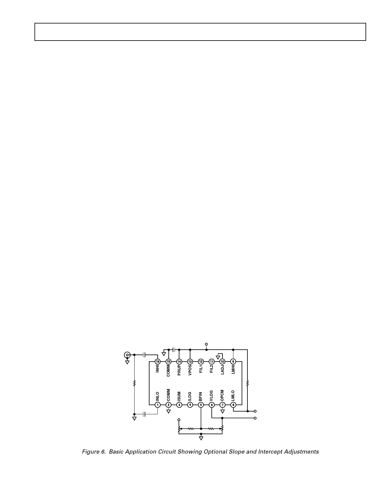
Basic RSSI Application
Figure 6 shows the basic RSSI (Receiver Signal Strength Indica-
tor) application circuit, including the calibration adjustments,
either or both of which may be omitted in noncritical applica-
tions. This circuit may be used “as is” in such measurement
applications as the log/IF strip in a spectrum or network ana-
lyzer or, with the addition of an FM or QPSK demodulator fed
by the limiter outputs, as an IF strip in such communications
applications as a GSM digital mobile radio or FM receiver.
The slope adjustment works in this way: the buffer amplifier
(which forms part of a Sallen-Key two-pole filter, see Figure 2)
has a dc gain of plus two, and the resistance from BFIN (buffer
in) to OPCM (output common) is nominally 9.375 kΩ. This
resistance is driven from the logarithmic detector sections with a
current scaled 2 µA/dB, generating 18.75 mV/dB at BFIN,
hence 37.5 mV/dB at VLOG Now, a resistor (R4 in Figure 6)
connected directly between BFIN and VLOG would form a
controlled positive-feedback network with the internal 9.375 kΩ
resistor which would raise the gain, and thus increase the slope
voltage, while the same external resistor connected between
BFIN and ground would form a shunt across the internal resis-
tor and reduce the slope voltage. By connecting R4 to a potenti-
ometer R2 across the output, the slope may be adjusted either
way; the value for R4 shown in Figure 6 provides approximately
± 10% range, with essentially no effect on the slope at the
midposition.
The intercept may be adjusted by adding a small current into
BFIN via R1 and R3. The AD606 is designed to have the nomi-
nal intercept value of –88 dBm when R1 is centered using this
network, which provides a range of ± 5 dB.
RF INPUT
100pF
0.1F
+5V
NC NC
51.1⍀
AD606
R5
200⍀
100pF
NC = NO CONNECT
+5V
R1
200k⍀
INTERCEPT
ADJUSTMENT
؎5dB
R3
412k⍀
R4
174k⍀
R2
50k⍀
SLOPE
ADJUSTMENT
؎10%
LIMITER OUTPUT
LOGARITHMIC
OUTPUT
Figure 6. Basic Application Circuit Showing Optional Slope and Intercept Adjustments
REV. B
–7–
Share Link: 