AD605(RevC) Просмотр технического описания (PDF) - Analog Devices
Номер в каталоге
Компоненты Описание
производитель
AD605 Datasheet PDF : 12 Pages
| |||
Two other easy combinations are possible to provide a gain
range of –14 dB to +82.8 dB: (1) make R1 a short and R2 an
open; or (2) make R1 an open and R2 a short. The bandwidth
for both of these cases will be dominated by the channel that is
set to the higher gain and will be about 8 MHz. From a noise
standpoint, the second choice is the best since by increasing the
gain of the first amplifier, the second amplifier’s noise will have
less of an impact on the total output noise. One further observa-
tion regarding noise is that by increasing the gain the output
noise will increase proportionally; therefore, there is no increase
in signal-to-noise ratio. It will actually stay fixed.
It should be noted that by selecting the appropriate values of R1
and R2, any gain range between –28 dB to +68.8 dB and 0 dB
to +96.8 dB can be achieved with the circuit in Figure 5. When
using any value other than shorts and opens for R1 and R2, the
final value of the gain range will depend on external resistors
matching on-chip resistors. Since the internal resistors can vary
by as much as ± 20%, the actual values for a particular gain have
to be determined empirically. Note that the two channels within
one part will match quite well; therefore, R1 will track R2 in
Figure 5.
C3 is not required since the common-mode voltage at Pin OUT1
should be identical to the one at Pins +IN2 and –IN2. However,
since only 1 mV of offset at the output of the first DSX will
introduce an offset of 53 mV when the second DSX is set to the
maximum gain of the lowest gain range (34.4 dB), and 263 mV
when set to the maximum gain of the highest gain range (48.4 dB),
it is important to include ac coupling to get the maximum dy-
namic range at the output of the cascaded amplifiers. C5 is
necessary if the output signal needs to be referenced to any
common-mode level other than half of the supply as is provided
by Pin OUT2.
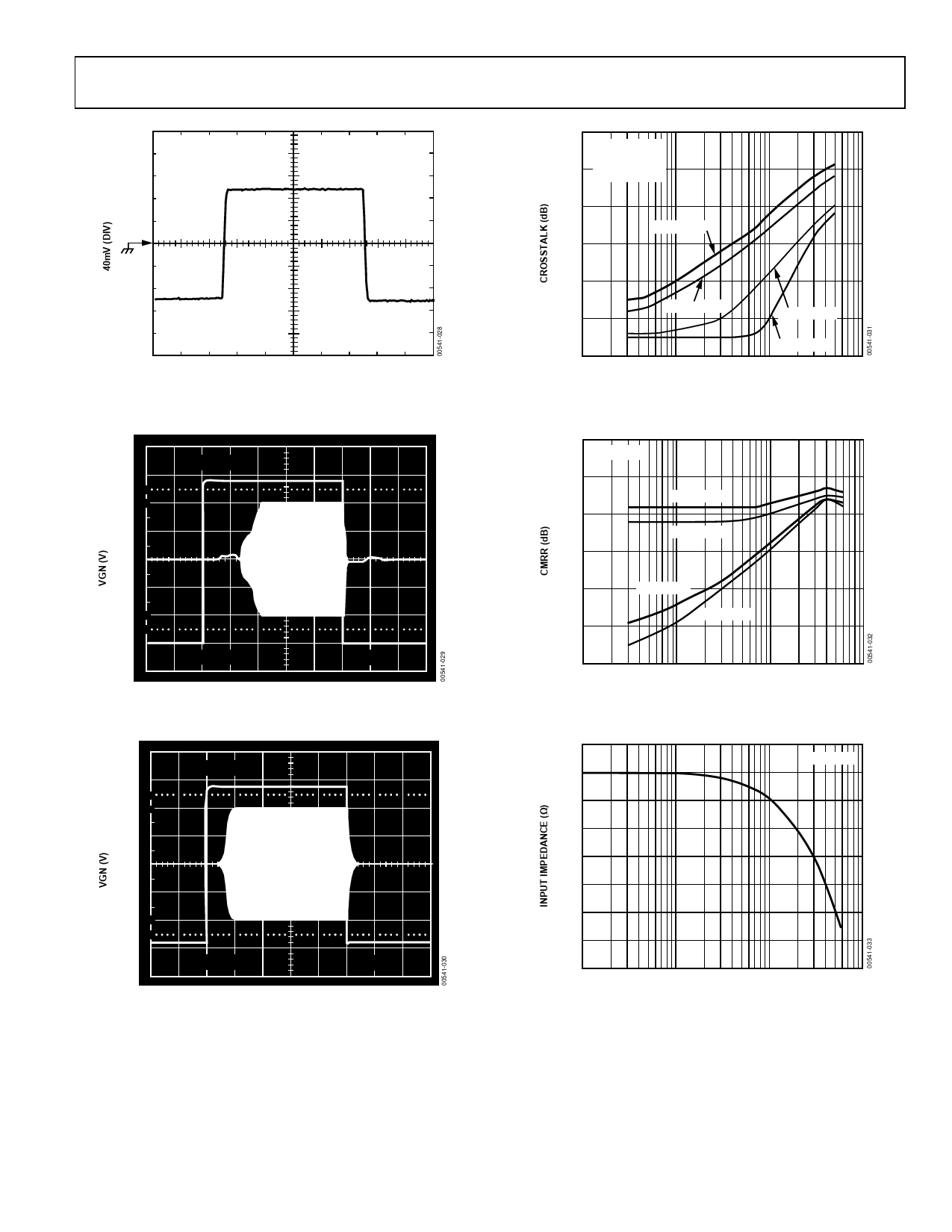
Figure 6 shows the gain versus VGN for the circuit in Figure 5
at 1 MHz and the lowest gain range (–14 dB to +34.4 dB). Note
that the gain scaling is 40 dB/V, double the 20 dB/V of an indi-
vidual DSX; this is the result of the parallel connection of the
gain control inputs, VGN1 and VGN2. One could of course
also sequentially increase the gain by first increasing the gain of
Channel 1 and then Channel 2. In that case VGN1 and VGN2
will have to be driven from separate voltage sources, for instance
two separate DACs. Figure 7 shows the gain error of Figure 5.
AD605
80
70
f = 1MHz
60
50
40
30
20
10
0
–10
–20
–30
–40
0.1
0.5
0.9
THEORETICAL
ACTUAL
1.3
1.7
2.1
2.5
2.9
VGN (V)
Figure 6. Gain vs. VGN for the Circuit in Figure 5
4
f = 1MHz
3
2
1
0
–1
–2
–3
–4
0.2
0.7
1.2
1.7
2.2
2.7
VGN (V)
Figure 7. Gain Error vs. VGN for the Circuit in Figure 5
REV. C
–11–
Share Link: 