AD602 Просмотр технического описания (PDF) - Analog Devices
Номер в каталоге
Компоненты Описание
производитель
AD602 Datasheet PDF : 32 Pages
| |||
AD600/AD602
THEORY OF OPERATION
The AD600/AD602 have the same general design and features.
They comprise two fixed gain amplifiers, each preceded by a
voltage-controlled attenuator of 0 dB to 42.14 dB with independent
control interfaces, each having a scaling factor of 32 dB per volt.
The AD600 amplifiers are laser trimmed to a gain of 41.07 dB
(×113), providing a control range of −1.07 dB to +41.07 dB
(0 dB to +40 dB with overlap). The AD602 amplifiers have a gain
of 31.07 dB (×35.8) and provide an overall gain of −11.07 dB to
+31.07 dB (−10 dB to +30 dB with overlap).
The advantage of this topology is that the amplifier can use
negative feedback to increase the accuracy of its gain. In
addition, because the amplifier does not have to handle large
signals at its input, the distortion can be very low. Another
feature of this approach is that the small-signal gain and phase
response, and thus the pulse response, are essentially
independent of gain.
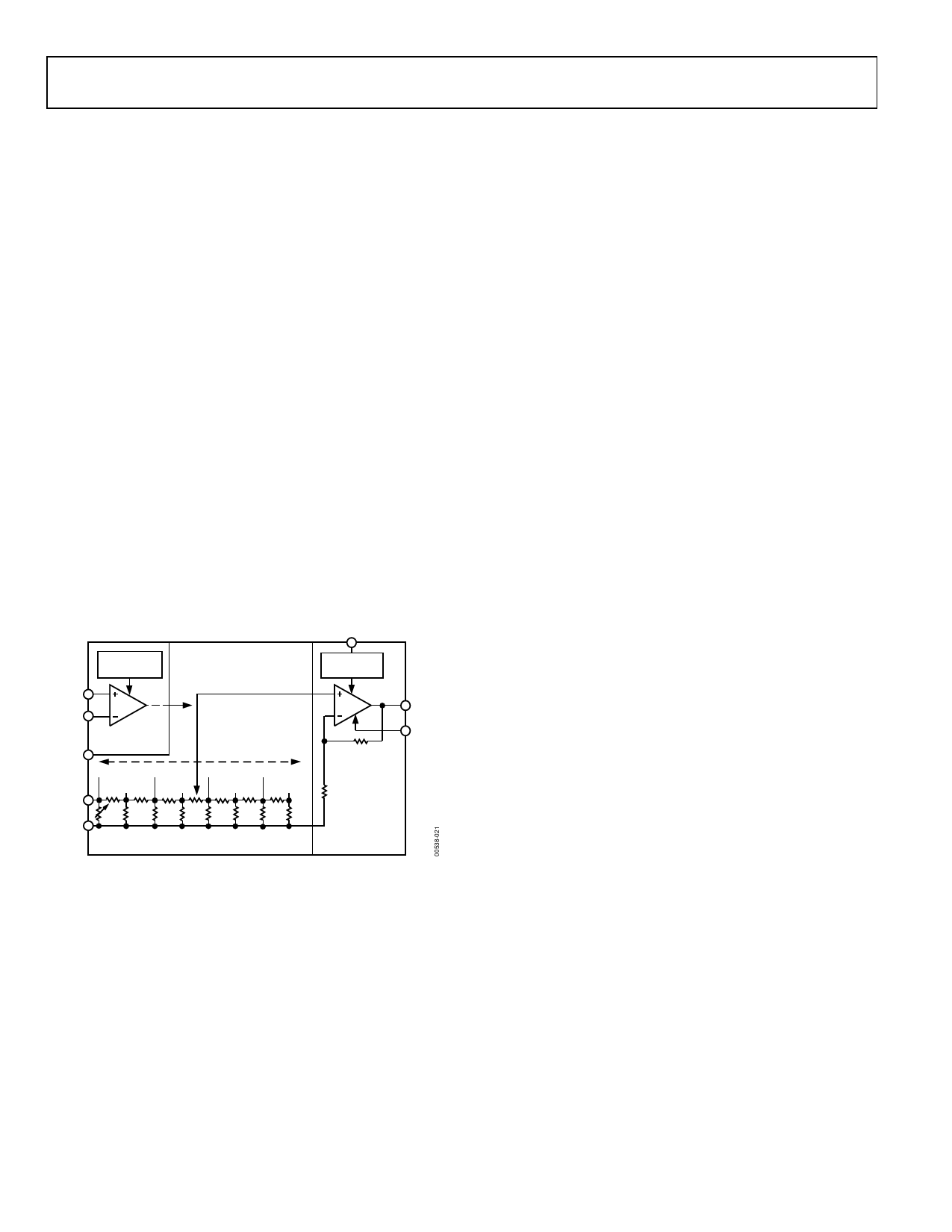
Figure 21 is a simplified schematic of one channel. The input
attenuator is a 7-stage R-2R ladder network, using untrimmed
resistors of nominally R = 62.5 Ω, which results in a characteristic
resistance of 125 Ω ± 20%. A shunt resistor is included at the
input and laser trimmed to establish a more exact input
resistance of 100 Ω ± 2%, which ensures accurate operation
(gain and HP corner frequency) when used in conjunction with
external resistors or capacitors.
GAT1
SCALING
REFERENCE
PRECISION PASSIVE
INPUT ATTENUATOR
GATING
INTERFACE
C1HI
C1LO
VG
GAIN CONTROL
INTERFACE
A1HI
0dB
–12.04dB
–22.08dB –36.12dB
–6.02dB –18.06dB
–30.1dB
–42.14dB
A1LO
500Ω
R-2R LADDER NETWORK
62.5Ω
A1OP
A1CM
RF2
2.24kΩ (AD600)
694Ω (AD602)
RF1
20Ω
FIXED-GAIN
AMPLIFIER
41.07dB (AD600)
31.07dB (AD602)
Figure 21. Simplified Block Diagram of a Single Channel of the AD600/AD602
The nominal maximum signal at input A1HI is 1 V rms (±1.4 V
peak) when using the recommended ±5 V supplies, although
operation to ±2 V peak is permissible with some increase in HF
distortion and feedthrough. Each attenuator is provided with a
separate signal LO connection for use in rejecting common
mode, the voltage between input and output grounds. Circuitry
is included to provide rejection of up to ±100 mV.
The signal applied at the input of the ladder network is
attenuated by 6.02 dB by each section; thus, the attenuation to
each of the taps is progressively 0 dB, 6.02 dB, 12.04 dB, 18.06 dB,
24.08 dB, 30.1 dB, 36.12 dB, and 42.14 dB. A unique circuit
technique is employed to interpolate between these tap points,
indicated by the slider in Figure 21, providing continuous
attenuation from 0 dB to 42.14 dB.
To understand the AD600/AD602, it helps to think in terms of
a mechanical means for moving this slider from left to right; in
fact, it is voltage controlled. The details of the control interface
are discussed later. Note that the gain is exactly determined at
all times and a linear decibel relationship is guaranteed auto-
matically between the gain and the control parameter that
determines the position of the slider. In practice, the gain
deviates from the ideal law by about ±0.2 dB peak (see Figure 28).
Note that the signal inputs are not fully differential. A1LO, A1CM
(for CH1), A2LO, and A2CM (for CH2) provide separate access
to the input and output grounds. This recognizes that, even when
using a ground plane, small differences arise in the voltages at
these nodes. It is important that A1LO and A2LO be connected
directly to the input ground(s). Significant impedance in these
connections reduces the gain accuracy. A1CM and A2CM
should be connected to the load ground(s).
NOISE PERFORMANCE
An important reason for using this approach is the superior
noise performance that can be achieved. The nominal resistance
seen at the inner tap points of the attenuator is 41.7 Ω (one third of
125 Ω), which, at 27°C, exhibits a Johnson noise spectral density
(NSD) of 0.84 nV/√Hz (that is, √4kTR), a large fraction of the
total input noise. The first stage of the amplifier contributes
another 1.12 nV/√Hz, for a total input noise of 1.4 nV/√Hz.
The noise at the 0 dB tap depends on whether the input is
short-circuited or open-circuited. When shorted, the minimum
NSD of 1.12 nV/√Hz is achieved. When open, the resistance of
100 Ω at the first tap generates 1.29 nV/√Hz, so the noise
increases to 1.71 nV/√Hz. This last calculation would be important
if the AD600 were preceded, for example, by a 900 Ω resistor to
allow operation from inputs up to ±10 V rms. However, in most
cases, the low impedance of the source limits the maximum
noise resistance.
Rev. F | Page 10 of 32
Share Link: 