AD5533BBCZ-1 Просмотр технического описания (PDF) - Analog Devices
Номер в каталоге
Компоненты Описание
производитель
AD5533BBCZ-1 Datasheet PDF : 16 Pages
| |||
AD5533B
TERMINOLOGY
VIN to VOUT Nonlinearity
This is a measure of the maximum deviation from a straight line
passing through the endpoints of the VIN versus VOUT transfer
function. It is expressed as a percentage of the full-scale span.
Total Unadjusted Error (TUE)
This is a comprehensive specification that includes relative accu-
racy, gain, and offset errors. It is measured by sampling a range
of voltages on VIN and comparing the measured voltages on
VOUT to the ideal value. It is expressed in mV.
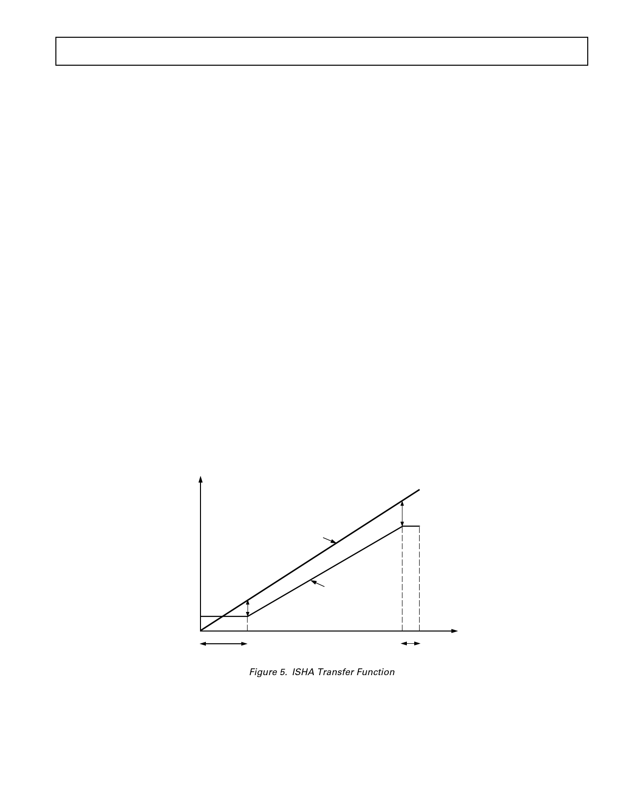
Offset Error
This is a measure of the output error when VIN = 70 mV. Ideally,
with VIN = 70 mV:
VOUT = (Gain × 70) − ((Gain − 1) × VOFFS_ IN ) mV
Offset error is a measure of the difference between VOUT (actual)
and VOUT (ideal). It is expressed in mV and can be positive or
negative. See Figure 5.
Gain Error
This is a measure of the span error of the analog channel. It is
the deviation in slope of the transfer function. See Figure 5. It is
calculated as:
Gain Error = Actual Full-Scale Output −
Ideal Full-Scale Output Offset − Error
where
Ideal Full-Scale Output = (Gain × 2.96) − ((Gain − 1) × VOFFS _ IN )
Ideal Gain = 3.52
Output Temperature Coefficient
This is a measure of the change in analog output with changes in
temperature. It is expressed in ppm/°C.
DC Power Supply Rejection Ratio
DC Power Supply Rejection Ratio (PSRR) is a measure of
the change in analog output for a change in supply voltage
(VDD and VSS). It is expressed in dBs. VDD and VSS are varied ±5%.
DC Crosstalk
This is the dc change in the output level of one channel in response
to a full-scale change in the output of all other channels. It is
expressed in µV.
Output Settling Time
This is the time taken from when BUSY goes high to when the
output has settled to ± 0.018%.
Acquisition Time
This is the time taken for the VIN input to be acquired. It is the
length of time that BUSY stays low.
OFFS_IN Settling Time
This is the time taken from a 0 V–3 V step change in input
voltage on OFFS_IN until the output has settled to within ± 0.39%.
Digital Feedthrough
This is a measure of the impulse injected into the analog outputs
from the digital control inputs when the part is not being written
to, i.e., CS/SYNC is high. It is specified in nV-secs and is measured
with a worst-case change on the digital input pins, e.g., from all
0s to all 1s and vice versa.
Output Noise Spectral Density
This is a measure of internally generated random noise. Random
noise is characterized as a spectral density (voltage per root Hertz).
It is measured by acquiring 1.5 V on all channels and measuring
noise at the output. It is measured in nV/√Hz typ.
AC Crosstalk
This is the area of the glitch that occurs on the output of one chan-
nel while another channel is acquiring. It is expressed in nV-secs.
VOUT
OFFSET
ERROR
IDEAL
TRANSFER
FUNCTION
ACTUAL
TRANSFER
FUNCTION
GAIN ERROR +
OFFSET ERROR
0V
70mV
LOWER
DEAD BAND
2.96 3V
VIN
UPPER
DEAD BAND
Figure 5. ISHA Transfer Function
REV. A
–9–
Share Link: 