AD534JDZ Просмотр технического описания (PDF) - Analog Devices
Номер в каталоге
Компоненты Описание
производитель
AD534JDZ Datasheet PDF : 20 Pages
| |||
AD534
PIN CONFIGURATIONS AND FUNCTION DESCRIPTIONS
+VS
X1
OUT
9
8
X2
10
AD534 7
1 TOP VIEW
Z1
(Not to 6 Z2
2
SF
Scale)
5
3
4
–VS
Y1
Y2
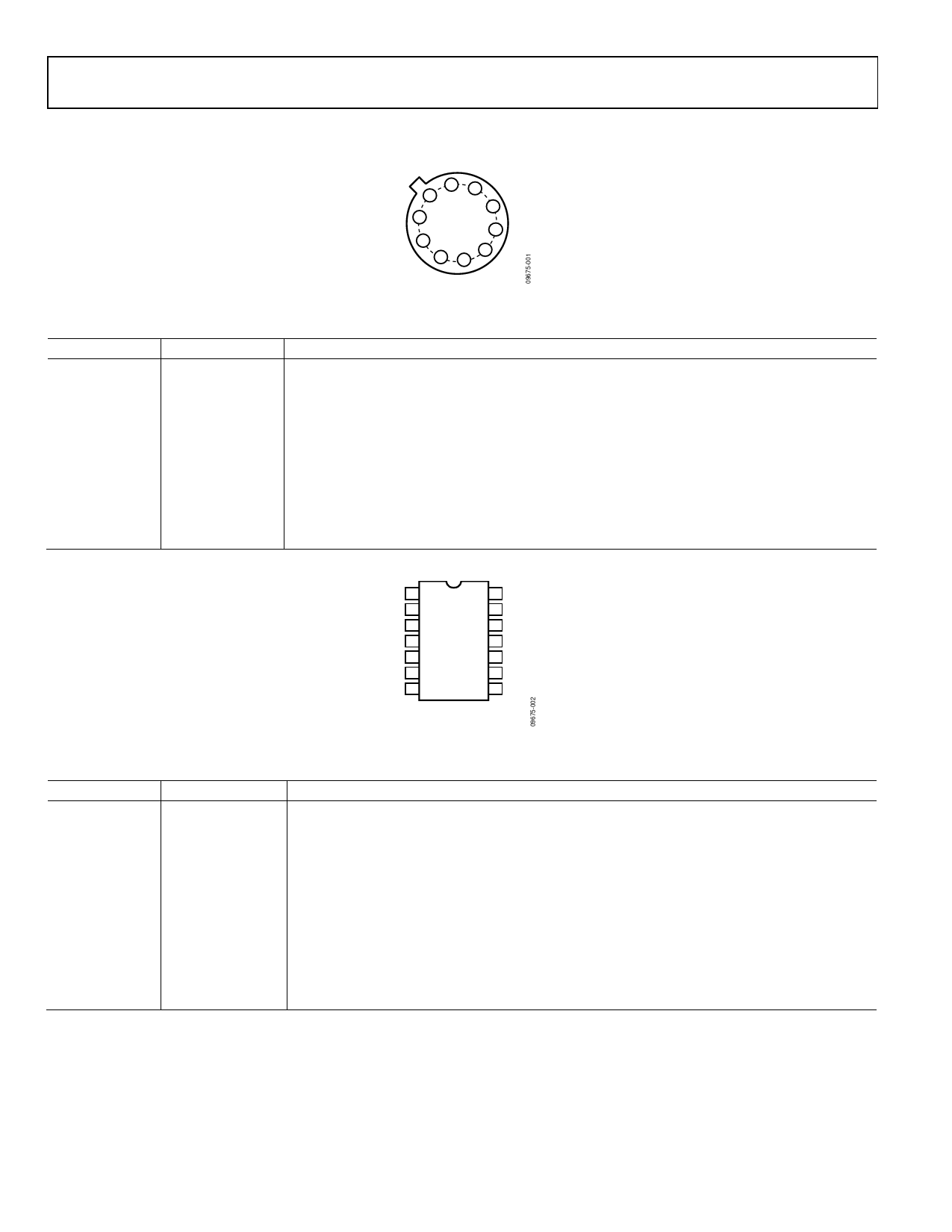
Figure 4. TO-100 (H-10) Pin Configuration
Table 5. H-10 Package Pin Function Descriptions
Pin No.
Mnemonic
Description
1
X2
Inverting Differential Input of the X Multiplicand Input.
2
SF
Scale Factor Input.
3
Y1
Noninverting Differential Input of the Y Multiplicand Input.
4
Y2
Inverting Differential Input of the Y Multiplicand Input.
5
−VS
Negative Supply Rail. Connects to header.
6
Z2
Inverting Differential Input of the Z Reference Input.
7
Z1
Noninverting Differential Input of the Z Reference Input.
8
OUT
Product Output.
9
+VS
Positive Supply Rail.
10
X1
Noninverting Differential Input of the X Multiplicand Input.
X1 1
X2 2
14 +VS
13 NC
NC 3 AD534 12 OUT
SF 4 TOP VIEW 11 Z1
NC 5 (Not to Scale) 10 Z2
Y1 6
9 NC
Y2 7
8 –VS
NC = NO CONNECT. DO NOT
CONNECT TO THIS PIN.
Figure 5. TO-100 (D-14) Pin Configuration
Table 6. D-14 Package Pin Function Descriptions
Pin No.
Mnemonic
Description
1
X1
Noninverting Differential Input of the X Multiplicand Input.
2
X2
Inverting Differential Input of the X Multiplicand Input.
3, 5, 9, 13
NC
No Connect. Do not connect to this pin.
4
SF
Scale Factor Input.
6
Y1
Noninverting Differential Input of the Y Multiplicand Input.
7
Y2
Inverting Differential Input of the Y Multiplicand Input.
8
−VS
Negative Supply Rail.
10
Z2
Inverting Differential Input of the Z Reference Input.
11
Z1
Noninverting Differential Input of the Z Reference Input.
12
OUT
Product Output.
14
+VS
Positive Supply rail.
Data Sheet
Rev. D | Page 8 of 20
Share Link: 