AD5342 Просмотр технического описания (PDF) - Analog Devices
Номер в каталоге
Компоненты Описание
производитель
AD5342 Datasheet PDF : 20 Pages
| |||
DB...11
DB0
CS
WR
A0
CLR
LDAC
AD5332/AD5333/AD5342/AD5343
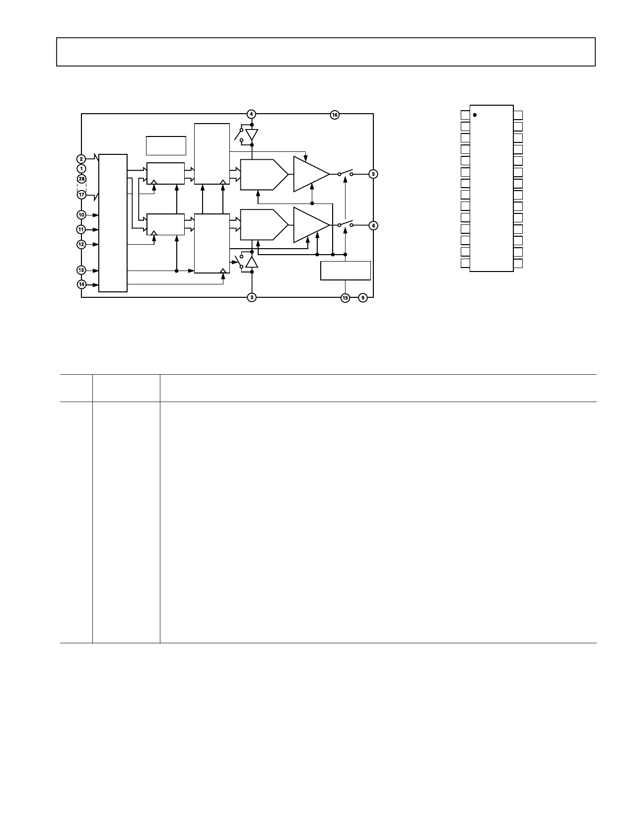
AD5342 FUNCTIONAL BLOCK DIAGRAM
AD5342 PIN CONFIGURATION
VREFA
POWER-ON
RESET
INPUT
REGISTER
DAC
REGISTER
INTER-
FACE
LOGIC
INPUT
REGISTER
DAC
REGISTER
RESET
12-BIT
DAC
12-BIT
DAC
VDD
AD5342
BUFFER
VOUTA
BUFFER
VOUTB
POWER-DOWN
LOGIC
GAIN 1
28 DB11
BUF 2
27 DB10
VREFB 3
26 DB9
VREFA 4
25 DB8
VOUTA 5
VOUTB 6
12-BIT
AD5342
24 DB7
23 DB6
NC 7 TOP VIEW 22 DB5
NC 8 (Not to Scale) 21 DB4
GND 9
20 DB3
CS 10
19 DB2
WR 11
18 DB1
A0 12
CLR 13
17 DB0
16 VDD
LDAC 14
15 PD
NC = NO CONNECT
VREFB
PD GND
Pin
No.
1
2
3
4
5
6
7, 8
9
10
11
12
13
14
15
16
17–28
Mnemonic
GAIN
BUF
VREFB
VREFA
VOUTA
VOUTB
NC
GND
CS
WR
A0
CLR
LDAC
PD
VDD
DB0–DB11
AD5342 PIN FUNCTION DESCRIPTIONS
Function
Gain Control Pin. This controls whether the output range from the DAC is 0-VREF or 0-2 VREF.
Buffer Control Pin. This pin controls whether the reference input to the DAC is buffered or unbuffered.
Reference Input for DAC B.
Reference Input for DAC A.
Output of DAC A. Buffered output with rail-to-rail operation.
Output of DAC B. Buffered output with rail-to-rail operation.
No Connect.
Ground reference point for all circuitry on the part.
Active Low Chip Select Input. This is used in conjunction with WR to write data to the parallel interface.
Active low Write Input. This is used in conjunction with CS to write data to the parallel interface.
Address pin for selecting between DAC A and DAC B.
Asynchronous active low control input that clears all input registers and DAC registers to zeros.
Active low control input that updates the DAC registers with the contents of the input registers. This
allows all DAC outputs to be simultaneously updated.
Power-Down Pin. This active low control pin puts all DACs into power-down mode.
Power Supply Pin. These parts can operate from 2.5 V to 5.5 V and the supply should be decoupled with a
10 F capacitor in parallel with a 0.1 F capacitor to GND.
12 Parallel Data Inputs. DB11 is the MSB of these 12 bits.
REV. 0
–7–
Share Link: 