ACT4060A Просмотр технического описания (PDF) - Unspecified
Номер в каталоге
Компоненты Описание
производитель
ACT4060A Datasheet PDF : 11 Pages
| |||
ACT4060A
Rev 0, 28-Apr-09
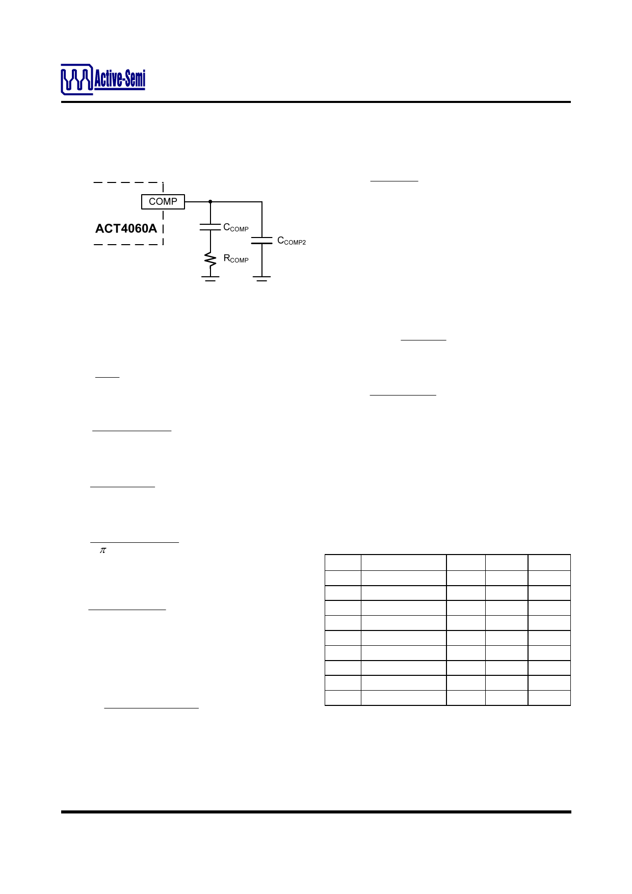
STABILITY COMPENSATION
Figure 2:
Stability Compensation
c: CCOMP2 is needed only for high ESR output capacitor
The feedback loop of the IC is stabilized by the
components at the COMP pin, as shown in Figure 2.
The DC loop gain of the system is determined by
the following equation:
AVDC
= 1.3V
IOUT
AVEA GCOMP
(4)
The dominant pole P1 is due to CCOMP:
fP1
=
G EA
2 π A VEA C COMP
(5)
The second pole P2 is the output pole:
fP 2
=
I OUT
2π VOUT C OUT
(6)
The first zero Z1 is due to RCOMP and CCOMP:
fZ1
=
1
2 π R COMP
C COMP
(7)
And finally, the third pole is due to RCOMP and
CCOMP2 (if CCOMP2 is used):
fP3
=
1
2πRCOMP CCOMP2
(8)
The following steps should be used to compensate
the IC:
STEP 1. Set the cross over frequency at 1/10 of the
switching frequency via RCOMP:
RCOMP
= 2πVOUT COUT fSW
10GEAGCOMP ×1.3V
= 1.7 ×10 8 VOUT COUT
(Ω)
(9)
but limit RCOMP to 15kΩ maximum.
STEP 2. Set the zero fZ1 at 1/4 of the cross over
frequency. If RCOMP is less than 15kΩ, the equation
for CCOMP is:
C COMP
= 1.8 × 10 −5
R COMP
(F)
(10)
If RCOMP is limited to 15kΩ, then the actual cross
over frequency is 3.4 / (VOUTCOUT). Therefore:
CCOMP =1.2 ×10⁻⁵VOUTCOUT
(F)
(11)
STEP 3. If the output capacitor’s ESR is high
enough to cause a zero at lower than 4 times the
cross over frequency, an additional compensation
capacitor CCOMP2 is required. The condition for using
CCOMP2 is:
RESRCOUT
≥
Min⎜⎜⎝⎛
1.1 ×10
COUT
−6
,0.012 ×VOUT
⎟⎟⎠⎞
(Ω)
(12)
And the proper value for CCOMP2 is:
CCOMP2
= C R OUT ESRCOUT
RCOMP
(13)
Though CCOMP2 is unnecessary when the output ca-
pacitor has sufficiently low ESR, a small value
CCOMP2 such as 100pF may improve stability against
PCB layout parasitic effects.
Table 2 shows some calculated results based on
the compensation method above.
Table 2:
Typical Compensation for Different Output
Voltages and Output Capacitors
VOUT
2.5V
3.3V
5V
2.5V
3.3V
5V
2.5V
3.3V
5V
COUT
RCOMP
22μF Ceramic 8.2kΩ
22μF Ceramic 12kΩ
22μF Ceramic 15kΩ
47μF SP CAP 15kΩ
47μF SP CAP 15kΩ
47μF SP CAP 15kΩ
470μF/6.3V/30mΩ 15kΩ
470μF/6.3V/30mΩ 15kΩ
470μF/6.3V/30mΩ 15kΩ
CCOMP CCOMP2c
2.2nF None
1.5nF None
1.5nF None
1.5nF None
1.8nF None
2.7nF None
15nF 1nF
22nF 1nF
27nF None
c: CCOMP2 is needed for high ESR output capacitor.
Figure 3 shows an example ACT4060A application circuit gener-
ating a 2.5V/2A output.
Innovative PowerTM
-6-
www.active-semi.com
Copyright © 2009 Active-Semi, Inc.
Share Link: 