ACS10D Просмотр технического описания (PDF) - Intersil
Номер в каталоге
Компоненты Описание
производитель
ACS10D Datasheet PDF : 8 Pages
| |||
Specifications ACS10MS
Absolute Maximum Ratings
Reliability Information
Supply Voltage (VCC). . . . . . . . . . . . . . . . . . . . . . . . . -0.5V to +6.0V
Input Voltage Range . . . . . . . . . . . . . . . . . . . . . .-0.5V to VCC +0.5V
DC Input Current, Any One Input . . . . . . . . . . . . . . . . . . . . . . . .±10mA
DC Drain Current, Any One Output. . . . . . . . . . . . . . . . . . . . . . .±50mA
Storage Temperature Range (TSTG) . . . . . . . . . . . -65oC to +150oC
Lead Temperature (Soldering 10s) . . . . . . . . . . . . . . . . . . . . +265oC
Junction Temperature (TJ) . . . . . . . . . . . . . . . . . . . . . . . . . . +175oC
ESD Classification . . . . . . . . . . . . . . . . . . . . . . . . . . . . . . . . Class 1
(All Voltages Reference to VSS)
Thermal Impedance
θJA
DIP. . . . . . . . . . . . . . . . . . . . . . . . . . . . . . 74oC/W
Flatpack . . . . . . . . . . . . . . . . . . . . . . . . . . 116oC/W
Maximum Package Power Dissipation at +125oC
θJC
24oC/W
30oC/W
DIP. . . . . . . . . . . . . . . . . . . . . . . . . . . . . . . . . . . . . . . . . . . . . 0.7W
Flatpack . . . . . . . . . . . . . . . . . . . . . . . . . . . . . . . . . . . . . . . . . 0.4W
Maximum Device Power Dissipation. . . . . . . . . . . . . . . . . . .(TBD)W
Gate Count . . . . . . . . . . . . . . . . . . . . . . . . . . . . . . . . . . . . . 42 Gates
CAUTION: As with all semiconductors, stress listed under “Absolute Maximum Ratings” may be applied to devices (one at a time) without resulting in permanent
damage. This is a stress rating only. Exposure to absolute maximum rating conditions for extended periods may affect device reliability. The conditions listed
under “Electrical Performance Characteristics” are the only conditions recommended for satisfactory device operation.
Operating Conditions
Supply Voltage . . . . . . . . . . . . . . . . . . . . . . . . . . . . . +4.5V to +5.5V
Input Rise and Fall Times at 4.5V VCC (TR, TF) . . . . . . 10ns/V Max
Operating Temperature Range (TA) . . . . . . . . . . . . -55oC to +125oC
Input High Voltage (VIH) . . . . . . . . . . . . . . . . . . VCC to 70% of VCC
Input Low Voltage (VIL). . . . . . . . . . . . . . . . . . . . .0V to 30% of VCC
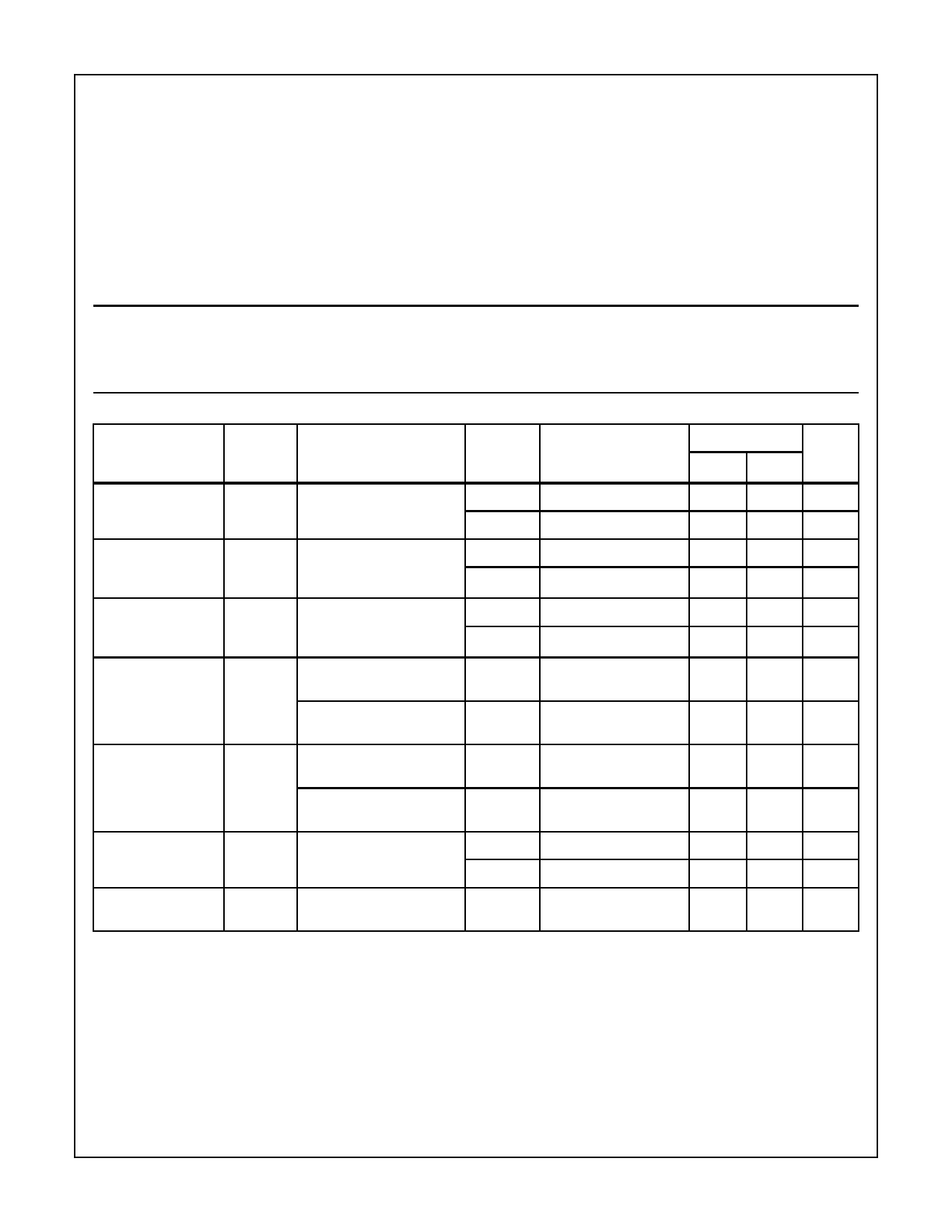
TABLE 1. DC ELECTRICAL PERFORMANCE CHARACTERISTICS
PARAMETER
Supply Current
SYMBOL
(NOTE 1)
CONDITIONS
ICC
VCC = 5.5V,
VIN = VCC or GND
Output Current
(Source)
Output Current
(Sink)
Output Voltage High
Output Voltage Low
Input Leakage
Current
IOH
IOL
VOH
VOL
IIN
VCC = VIH = 4.5V,
VOUT = VCC -0.4V,
VIL = 0V, (Note 2)
VCC = VIH = 4.5V,
VOUT = 0.4V, VIL = 0V,
(Note 2)
VCC = 5.5V, VIH = 3.85V
VIL = 1.65V, IOH = -50µA
VCC = 4.5V, VIH = 3.15V,
VIL = 1.35V, IOH = -50µA
VCC = 5.5V, VIH = 3.85V
VIL = 1.65V, IOH = 50µA
VCC = 4.5V, VIH = 3.15V,
VIL = 1.35V, IOH = 50µA
VCC = 5.5V,
VIN = VCC or GND
Noise Immunity
Functional Test
FN
VCC = 4.5V, VIH = 3.15V,
VIL = 1.35V, (Note 3)
GROUP
A SUB-
GROUPS
1
2, 3
1
2, 3
1
2, 3
1, 2, 3
LIMITS
TEMPERATURE
+25oC
+125oC, -55oC
+25oC
+125oC, -55oC
MIN MAX
-
5
-
100
-12
-
-8
-
+25oC
+125oC, -55oC
12
-
8
-
+25oC, +125oC, -55oC VCC -0.1 -
1, 2, 3
+25oC, +125oC, -55oC VCC -0.1 -
1, 2, 3
+25oC, +125oC, -55oC
-
0.1
1, 2, 3
+25oC, +125oC, -55oC
-
0.1
1
+25oC
-
2, 3
+125oC, -55oC
-
7, 8A, 8B +25oC, +125oC, -55oC
-
±0.5
±1.0
-
NOTE:
1. All voltages referenced to device GND.
2. Force/measure functions may be interchanged.
3. For functional tests, VO ≥4.0V is recognized as a logic “1”, and VO ≤0.5V is recognized as a logic “0”.
UNITS
µA
µA
mA
mA
mA
mA
V
V
V
V
µA
µA
V
Spec Number 518814
2
Share Link: 