ACPL-P454-500E Просмотр технического описания (PDF) - Avago Technologies
Номер в каталоге
Компоненты Описание
производитель
ACPL-P454-500E Datasheet PDF : 9 Pages
| |||
Package Characteristics
Over recommended temperature (TA = 0°C to 70°C) unless otherwise specified. All typicals at TA = 25°C.
Parameter
Symbol Min. Typ. Max. Units Test Conditions
Fig. Note
Input-Output Momentary VISO
3750
Vrms RH d 50%, t = 1 min, TA = 25°C
6,12
Withstand Voltage*
5000 (For “ACPL-W454)
Input-Output Resistance
RI-O
1012
:
VI-O = 500 Vdc
6
Input-Output Capacitance CI-O
0.6
pF
f = 1 MHz; VI-O = 0 Vdc
6
* The Input-Output Momentary Withstand Voltage is a dielectric voltage rating that should not be interpreted as an input-output continuous voltage
rating. For the continuous voltage rating refer to the IEC/EN/DIN EN 60747-5-2 Insulation Characteristics Table (if applicable).
Notes:
1. Derate linearly above 70°C free-air temperature at a rate of 0.8 mA/°C.
2. Derate linearly above 70°C free-air temperature at a rate of 1.6mA/°C.
3. Derate linearly above 70°C free-air temperature at a rate of 0.9 mW/°C.
4. Derate linearly above 70°C free-air temperature at a rate of 2.0 mW/°C.
5. CURRENT TRANSFER RATIO in percent is defined as the ratio of output collector current (IO), to the forward LED input current (IF), times 100.
6. Device considered a two-terminal device: Pins 1 and 3 shorted together and Pins 4, 5 and 6 shorted together.
7. Under TTL load and drive conditions: Common mode transient immunity in a Logic High level is the maximum tolerable (positive) dVCM/dt on the
leading edge of the common mode pulse, VCM, to assure that the output will remain in a Logic High state (i.e., VO > 2.0 V). Common mode transient
immunity in a Logic Low level is the maximum tolerable (negative) dVCM/dt on the trailing edge of the common mode pulse signal, VCM, to assure
that the output will remain in a Logic Low state (i.e., VO < 0.8 V).
8. Under IPM (Intelligent Power Module) load and LED drive conditions: Common mode transient immunity in a Logic High level is the maximum
tolerable dVCM/dt on the leading edge of the common mode pulse, VCM, to assure that the output will remain in a Logic High state (i.e., VO > 3.0
V). Common mode transient immunity in a Logic Low level is the maximum tolerable dVCM/dt on the trailing edge of the common mode pulse
signal,VCM, to assure that the output will remain in a Logic Low state (i.e., VO < 1.0 V).
9. The 1.9 k: load represents 1 TTL unit load of 1.6 mA and the 5.6 k: pull-up resistor.
10. The RL = 20 k:, CL = 100 pF load represents an IPM (Intelligent Power Mode) load.
11. Use of a 0.1 PF bypass capacitor connected between pins 4 and 6 is recommended.
12. In accordance with UL 1577, each optocoupler is proof tested by applying an insulation test voltage t 4500 VRMS for 1 second (leakage detection
current limit, II-O d 5 PA); each optocoupler under ACPL-W454 is proof tested by applying an insulation test voltage ≥ 6000 VRMS for 1 second (leak-
age detection current limit, II-O ≤ 5 μA).
13. The difference between tPLH and tPHL, between any two ACPL-W454/P454 parts under the same test condition. (See Power Inverter Dead Time and
Propagation Delay Specifications section).
TA = 25 ˚C
10 VCC = 5.0 V
40 mA
35 mA
30 mA
25 mA
5
20 mA
15 mA
10 mA
IF = 5 mA
0
0
10
20
V O - OUTPUT VOLTAGE - V
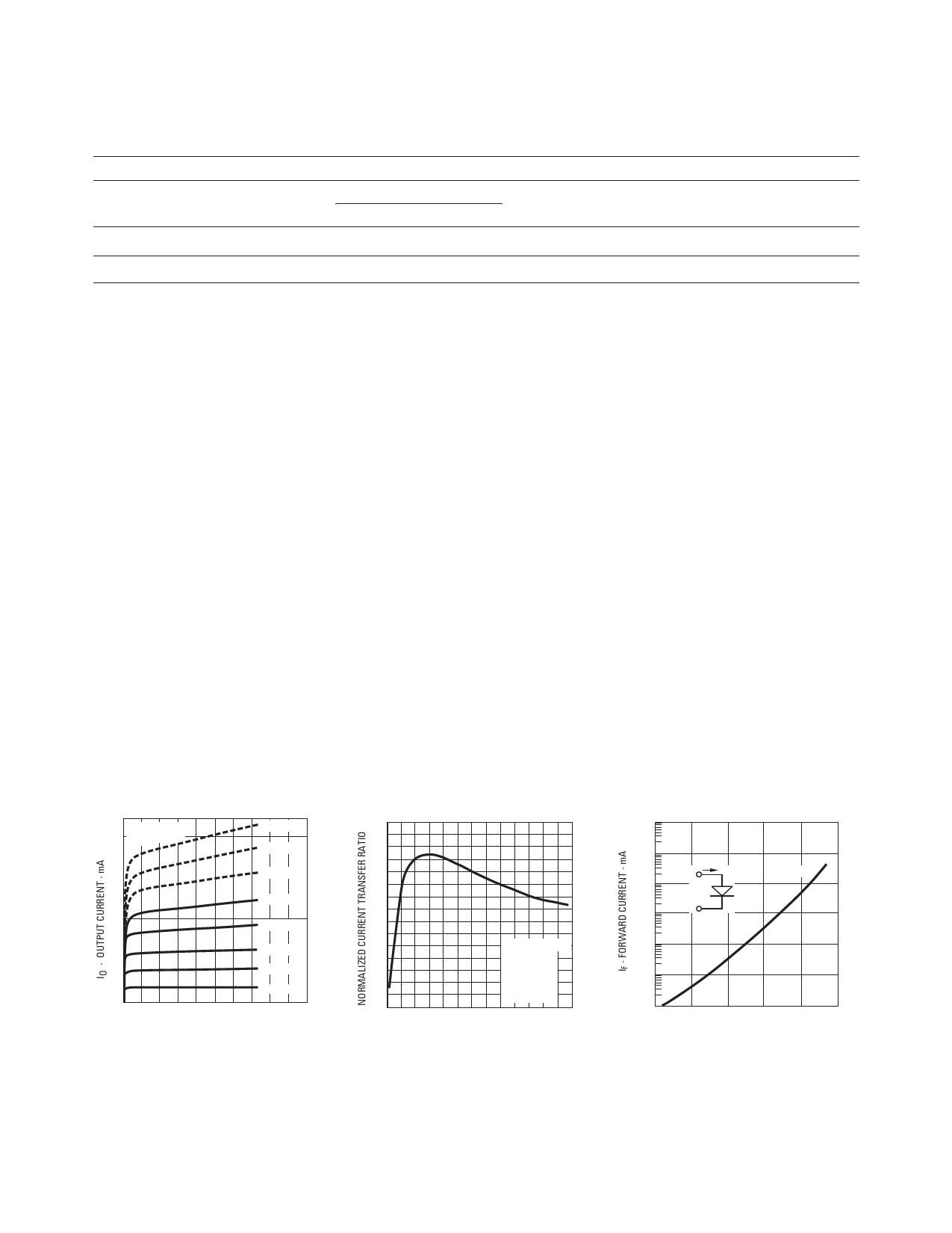
Figure 1. DC and Pulsed Transfer Characteristics.
1.5
1000
100
IF
TA = 25˚C
1.0
10
+
VF
-
1.0
0.5
NORMALIZED
IF = 16 mA
V O = 0.4 V
V CC = 5.0 V
T A = 25 ˚C
0.0
0 2 4 6 8 10 12 14 16 18 20 22 24 26
IF - INPUT CURRENT - mA
Figure 2. Current Transfer Ratio vs. Input Current.
0.1
0.01
0.001
1.1
1.2
1.3 1.4
1.5
1.6
VF - FORWARD VOLTAGE - VOLTS
Figure 3. Input Current vs. Forward Voltage.
7
Share Link: 