ACPL-796J Просмотр технического описания (PDF) - Avago Technologies
Номер в каталоге
Компоненты Описание
производитель
ACPL-796J Datasheet PDF : 16 Pages
| |||
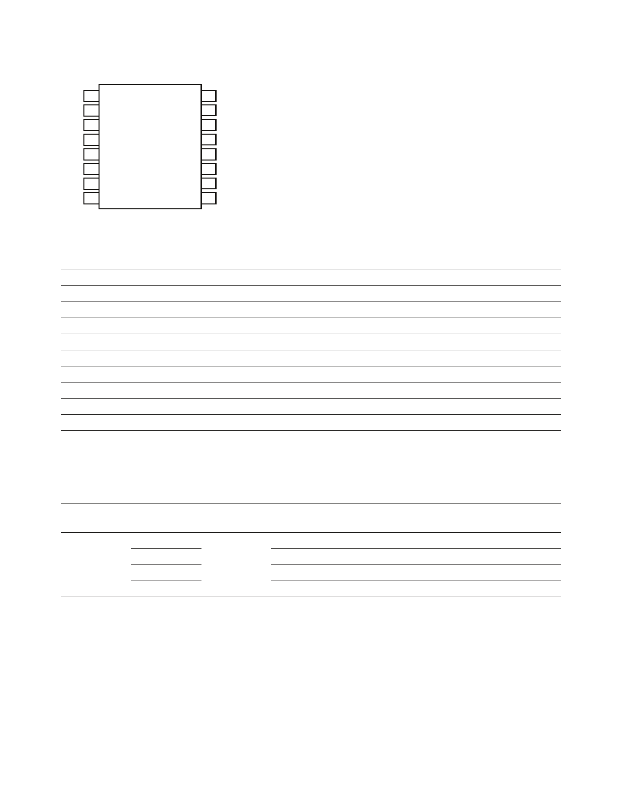
Pin Configuration and Descriptions
VDD1 1
VIN+ 2
VIN– 3
GND1 4
NC 5
NC 6
VDD1 7
GND1 8
ACPL-796J
16 GND2
15 NC
14 VDD2
13 MCLKIN
12 NC
11 MDAT
10 NC
9 GND2
Figure 2. Pin configuration.
Table 1. Pin descriptions.
Pin No.
Symbol
1, 7
VDD1
2
VIN+
3
VIN–
4, 8
GND1
5, 6, 10, 12, 15
NC
9, 16
GND2
11
MDAT
13
MCLKIN
14
VDD2
Description
Supply voltage for signal input side (analog side), relative to GND1
Positive analog input, recommended input range ±200 mV
Negative analog input, recommended input range ±200 mV (normally connected to GND1)
Supply ground for signal input side
No connection. Leave floating
Supply ground for data output side (digital side)
Modulator data output
Modulator clock input, 5 MHz to 20 MHz
Supply voltage for data output side, relative to GND2
Table 2. Ordering Information
ACPL-796J is UL recognized with 5000 Vrms/1 minute rating per UL 1577.
Part number
ACPL-796J
Option
(RoHS Compliant)
-000E
-060E
-500E
-560E
Package
SO-16
Surface Mount
X
X
X
X
Tape& Reel
X
X
IEC/EN/DIN EN
60747-5-5
X
X
Quantity
45 per tube
45 per tube
850 per reel
850 per reel
To order, choose a part number from the part number column and combine with the desired option from the option
column to form an order entry.
Example:
ACPL-796J-560E to order product of Surface Mount package in Tape and Reel packaging with IEC/EN/DIN EN 60747-5-5
Safety Approval and RoHS compliance.
Option datasheets are available. Contact your Avago sales representative or authorized distributor for information.
2
Share Link: 