H1115I Просмотр технического описания (PDF) - Intersil
Номер в каталоге
Компоненты Описание
производитель
H1115I Datasheet PDF : 14 Pages
| |||
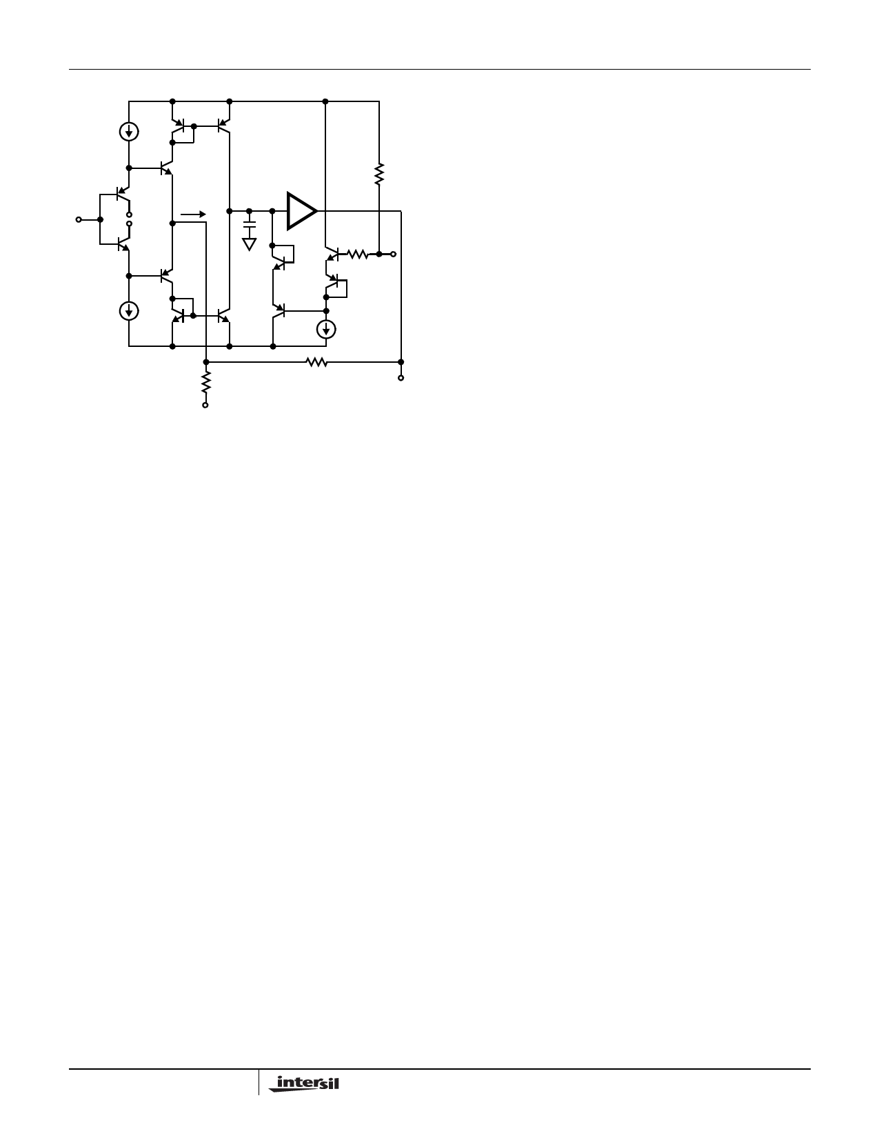
HFA1115
QP3
V+
QP4
QN2
R1 50kΩ
+IN
QP1
V-
ILIMIT
Z
+1
V+
QN1
QP2
QN5
QN6
QP6
200Ω VH
QN3
QN4 QP5
V-
V-IN
RG = 350Ω
RF = 350Ω
(INTERNAL) (INTERNAL)
-IN
VOUT
FIGURE 3. HFA1115 SIMPLIFIED VH LIMIT CIRCUITRY
This current is mirrored onto the high impedance node (Z) by
QX3-QX4, where it is converted to a voltage and fed to the
output via another unity gain buffer. If no limiting is utilized,
the high impedance node may swing within the limits defined
by QP4 and QN4. Note that when the output reaches its
quiescent value, the current flowing through -IN is reduced
to only that small current (-IBIAS) required to keep the output
at the final voltage.
Tracing the path from VH to Z illustrates the effect of the limit
voltage on the high impedance node. VH decreases by 2VBE
(QN6 and QP6) to set up the base voltage on QP5. QP5
begins to conduct whenever the high impedance node
reaches a voltage equal to QP5’s base voltage + 2VBE (QP5
and QN5). Thus, QP5 limits node Z whenever Z reaches VH.
R1 provides a pull-up network to ensure functionality with the
limit inputs floating. A similar description applies to the
symmetrical low limit circuitry controlled by VL.
When the output is limited, the negative input continues to
source a slewing current (ILimit) in an attempt to force the
output to the quiescent voltage defined by the input. QP5
must sink this current while limiting, because the -IN current
is always mirrored onto the high impedance node. The
limiting current is calculated as:
ILIMIT = (V-IN - VOUT LIMITED)/RF + V-IN/RG.
As an example, a unity gain circuit with VIN = 2V, and VH = 1V,
would have ILIMIT = (2V - 1V)/350Ω + 2V/∞ = 2.8mA (RG = ∞
because -IN is floated for unity gain applications). Note that ICC
increases by ILIMIT when the output is limited.
Limit Accuracy
The limited output voltage will not be exactly equal to the
voltage applied to VH or VL. Offset errors, mostly due to VBE
mismatches, necessitate a limit accuracy parameter which is
found in the device specifications. Limit accuracy is a
function of the limiting conditions. Referring again to Figure
3, it can be seen that one component of limit accuracy is the
VBE mismatch between the QX6 transistors, and the QX5
transistors. If the transistors always ran at the same current
level there would be no VBE mismatch, and no contribution
to the inaccuracy. The QX6 transistors are biased at a
constant current, but as described earlier, the current
through QX5 is equivalent to ILimit . VBE increases as ILIMIT
increases, causing the limited output voltage to increase as
well. ILIMIT is a function of the overdrive level
((AV x VIN - VLIMIT) / VLIMIT), so limit accuracy degrades as
the overdrive increases (see Figures 28 and 29). For
example, accuracy degrades from -20mV to +30mV when
the overdrive increases from 100% to 200% (AV = +2,
VH = 500mV).
Consideration must also be given to the fact that the limit
voltages have an effect on amplifier linearity. The “Linearity
Near Limit Voltage” curves, Figures 30 and 31, illustrate the
impact of several limit levels on linearity.
Limit Range
Unlike some competitor devices, both VH and VL have
usable ranges that cross 0V. While VH must be more
positive than VL, both may be positive or negative, within
the range restrictions indicated in the specifications. For
example, the HFA1115 could be limited to ECL output
levels by setting VH = -0.8V and VL = -1.8V. VH and VL
may be connected to the same voltage (GND for instance)
but the result won’t be a DC output voltage from an AC
input signal. A 150mV - 200mV AC signal will still be
present at the output.
Recovery from Overdrive
The output voltage remains at the limit level as long as the
overdrive condition remains. When the input voltage drops
below the overdrive level (VLIMIT/AV) the amplifier returns to
linear operation. A time delay, known as the Overdrive
Recovery Time, is required for this resumption of linear
operation. Overdrive recovery time is defined as the
difference between the amplifier’s propagation delay exiting
limiting and the amplifier’s normal propagation delay, and it
is a strong function of the overdrive level. Figure 32 details
the overdrive recovery time for various limit and overdrive
levels
Benefits of Output Limiting
The plots of “Pulse Response Without Limiting” and “Pulse
Response With Limiting” (Figures 4 and 5) highlight the
advantages of output limiting. Besides the obvious benefit of
constraining the output swing to a defined range, limiting the
output excursions also keeps the output transistors from
saturating, which prevents unwanted saturation artifacts
from distorting the output signal. Output limiting also takes
advantage of the HFA1115’s ultra-fast overdrive recovery
7
Share Link: 