VT16245BDGG Просмотр технического описания (PDF) - Philips Electronics
Номер в каталоге
Компоненты Описание
производитель
VT16245BDGG Datasheet PDF : 10 Pages
| |||
Philips Semiconductors
3.3V 16-bit transceiver (3-State)
Product specification
74LVT16245B
FEATURES
• 16-bit bidirectional bus interface
• 3-State buffers
• Output capability: +64mA/-32mA
• TTL input and output switching levels
• Input and output interface capability to systems at 5V supply
• Bus-hold data inputs eliminate the need for external pull-up
resistors to hold unused inputs
• Live insertion/extraction permitted
• Power-up 3-State
• No bus current loading when output is tied to 5V bus
• Latch-up protection exceeds 500mA per JEDEC Std 17
• ESD protection exceeds 2000V per MIL STD 883 Method 3015
and 200V per Machine Model
DESCRIPTION
The 74LVT16245B is a high-performance BiCMOS product
designed for VCC operation at 3.3V.
This device is a 16-bit transceiver featuring non-inverting 3-State
bus compatible outputs in both send and receive directions. The
control function implementation minimizes external timing
requirements. The device features an Output Enable (OE) input for
easy cascading and a Direction (DIR) input for direction control.
QUICK REFERENCE DATA
SYMBOL
PARAMETER
tPLH
tPHL
CIN
CI/O
ICCZ
Propagation delay
nAx to nBx or nBx to nAx
Input capacitance DIR, OE
I/O pin capacitance
Total supply current
CONDITIONS
Tamb = 25°C
CL = 50pF;
VCC = 3.3V
VI = 0V or 3.0V
VI/O = 0V or 3.0V
Outputs disabled; VCC = 3.6V
TYPICAL
1.9
3
9
70
UNIT
ns
pF
pF
µA
ORDERING INFORMATION
PACKAGES
48-Pin Plastic SSOP Type III
48-Pin Plastic TSSOP Type II
TEMPERATURE RANGE
–40°C to +85°C
–40°C to +85°C
OUTSIDE NORTH AMERICA
74LVT16245B DL
74LVT16245B DGG
NORTH AMERICA
VT16245B DL
VT16245B DGG
DWG NUMBER
SOT370-1
SOT362-1
PIN DESCRIPTION
PIN NUMBER SYMBOL
NAME AND FUNCTION
1, 24
nDIR Direction control input
47, 46, 44, 43,
41, 40, 38, 37,
36, 35, 33, 32,
30, 29, 27, 26
nA0 – nA7 Data inputs/outputs (A side)
2, 3, 5, 6, 8, 9,
11, 12, 13, 14,
16, 17, 19, 20,
22, 23
nB0 – nB7 Data inputs/outputs (B side)
25, 48
nOE
Output enable input
(active-Low)
4, 10, 15, 21, 28,
34, 39, 45
GND Ground (0V)
7, 18, 31, 42
VCC
Positive supply voltage
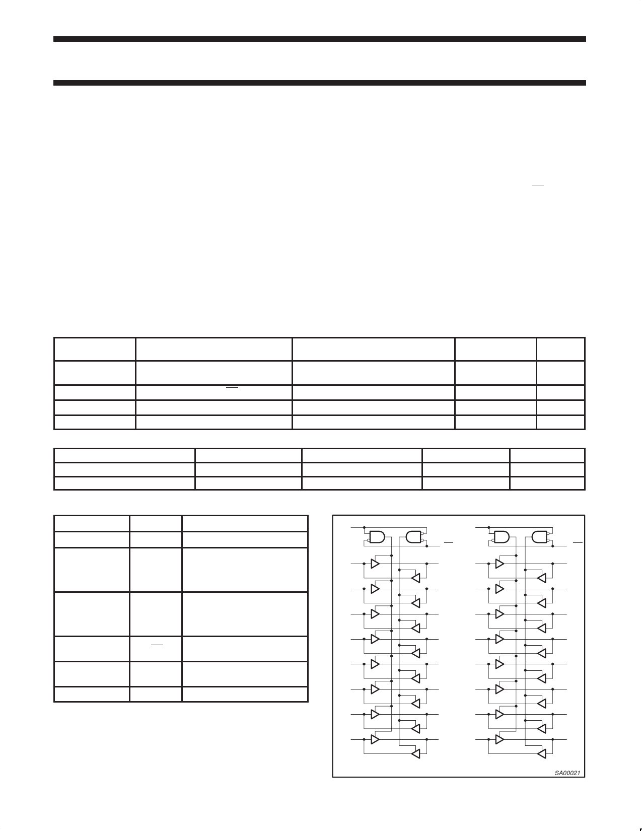
LOGIC SYMBOL
1
1DIR
1A0 47
1A1 46
1A2 44
1A3 43
1A4 41
1A5 40
1A6 38
2DIR 24
48 1OE
2 1B0 2A0 36
3 1B1 2A1 35
5 1B2 2A2 33
6 1B3 2A3 32
8 1B4 2A4 30
9 1B5 2A5 29
11 1B6 2A6 27
25 2OE
13 2B0
14 2B1
16 2B2
17 2B3
19 2B4
20 2B5
22 2B6
1A7 37
12 1B7 2A7 26
23 2B7
1998 Feb 19
SA00021
2
853-1753 18990
Share Link: 