74LVC245A(2004) Просмотр технического описания (PDF) - STMicroelectronics
Номер в каталоге
Компоненты Описание
производитель
74LVC245A
(Rev.:2004)
(Rev.:2004)
STMicroelectronics

74LVC245A Datasheet PDF : 12 Pages
| |||
74LVC245A
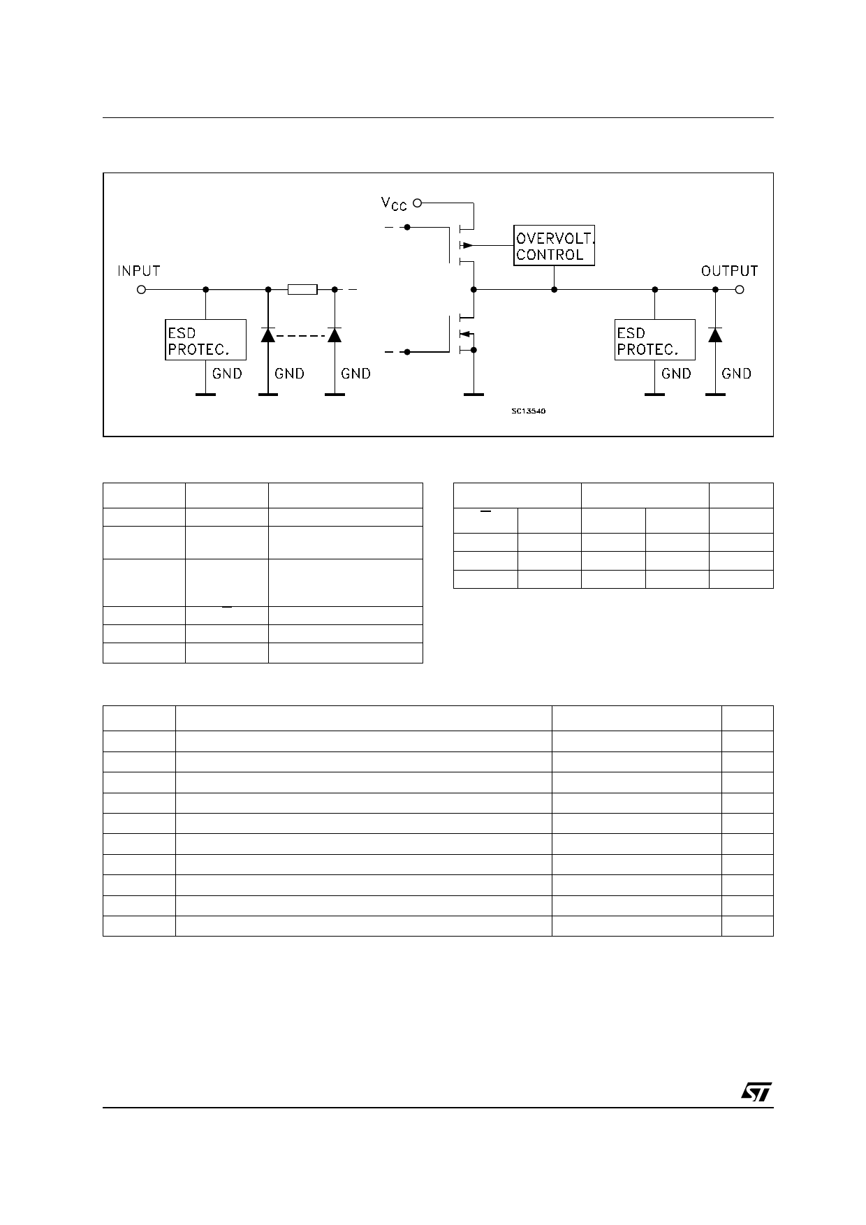
Figure 2: Input And Output Equivalent Circuit
Table 2: Pin Description
Table 3: Truth Table
PIN N°
1
2, 3, 4, 5, 6,
7, 8, 9
18, 17, 16,
15, 14, 13,
12, 11
19
10
20
SYMBOL
DIR
A1 to A8
NAME AND FUNCTION
Directional Control
Data Inputs/Outputs
B1 to B8 Data Inputs/Outputs
G
GND
VCC
Output Enable Input
Ground (0V)
Positive Supply Voltage
Table 4: Absolute Maximum Ratings
INPUTS
G
DIR
L
L
L
H
H
X
X : Don’t Care
Z : High Impedance
FUNCTION
OUTPUT
A BUS B BUS
OUTPUT INPUT
INPUT OUTPUT
Z
Z
Yn
A=B
B=A
Z
Symbol
Parameter
VCC Supply Voltage
VI
DC Input Voltage
VO
DC Output Voltage (High Impedance or VCC = 0V)
VO
DC Output Voltage (High or Low State) (note 1)
IIK
DC Input Diode Current
IOK
DC Output Diode Current (note 2)
IO
DC Output Current
ICC or IGND DC VCC or Ground Current per Supply Pin
Tstg Storage Temperature
TL
Lead Temperature (10 sec)
Value
Unit
-0.5 to +7.0
V
-0.5 to +7.0
V
-0.5 to +7.0
V
-0.5 to VCC + 0.5
V
- 50
mA
- 50
mA
± 50
mA
± 100
mA
-65 to +150
°C
300
°C
Absolute Maximum Ratings are those values beyond which damage to the device may occur. Functional operation under these conditions is
not implied
1) IO absolute maximum rating must be observed
2) VO < GND
2/12
Share Link: