74LV132 Просмотр технического описания (PDF) - Philips Electronics
Номер в каталоге
Компоненты Описание
производитель
74LV132 Datasheet PDF : 12 Pages
| |||
Philips Semiconductors
Quad 2-input NAND Schmitt-trigger
Product specification
74LV132
FEATURES
• Wide operating voltage: 1.0 to 5.5V
• Optimized for Low Voltage applications: 1.0 to 3.6V
• Accepts TTL input levels between VCC = 2.7V and VCC = 3.6V
• Typical VOLP (output ground bounce) t 0.8V @ VCC = 3.3V,
Tamb = 25°C
• Typical VOHV (output VOH undershoot) u 2V @ VCC = 3.3V,
Tamb = 25°C
• Output capability: standard
• ICC category: SSI
APPLICATIONS
• Wave and pulse shapers
• Astable multivibrators
• Monostable multivibrators
DESCRIPTION
The 74LV132 is a low-voltage Si-gate CMOS device and is pin and
function compatible with 74HC/HCT132.
The 74LV132 contains four 2-input NAND gates which accept
standard input signals. They are capable of transforming slowly
changing input signals into sharply defined, jitter-free output signals.
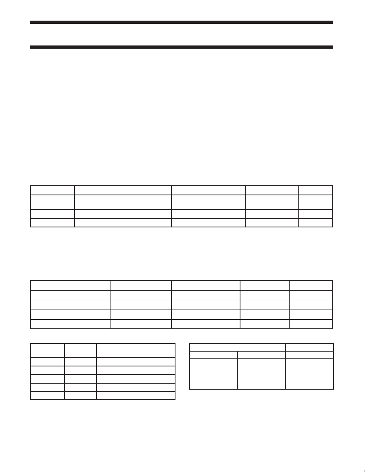
QUICK REFERENCE DATA
GND = 0V; Tamb = 25°C; tr = tf v2.5 ns
SYMBOL
PARAMETER
The gate switches at different points for positive and negative-going
signals. The difference between the positive voltage VT+ and the
negative voltage VT– is defined as the hysteresis voltage VH.
CONDITIONS
TYPICAL
UNIT
tPHL/tPLH
Propagation delay
nA, nB to nY
CL = 15pF
VCC = 3.3V
CI
Input capacitance
CPD
Power dissipation capacitance per gate
Notes 1 and 2
NOTES:
1. CPD is used to determine the dynamic power dissipation (PD in µW)
PD = CPD VCC2 fi )S (CL VCC2 fo) where:
fi = input frequency in MHz; CL = output load capacitance in pF;
fo = output frequency in MHz; VCC = supply voltage in V;
S (CL VCC2 fo) = sum of the outputs.
2. The condition is VI = GND to VCC
10
ns
3.5
pF
24
pF
ORDERING INFORMATION
PACKAGES
14-Pin Plastic DIL
14-Pin Plastic SO
14-Pin Plastic SSOP Type II
14-Pin Plastic TSSOP Type I
TEMPERATURE RANGE OUTSIDE NORTH AMERICA
–40°C to +125°C
74LV132 N
–40°C to +125°C
74LV132 D
–40°C to +125°C
74LV132 DB
–40°C to +125°C
74LV132 PW
NORTH AMERICA
74LV132 N
74LV132 D
74LV132 DB
74LV132PW DH
PKG. DWG. #
SOT27-1
SOT108-1
SOT337-1
SOT402-1
PIN DESCRIPTION
PIN
NUMBER
SYMBOL
1, 4, 9, 12
1A to 4A
2, 5, 10, 13
1B to 4B
3, 6, 8, 11
1Y to 4Y
7
GND
14
VCC
FUNCTION
Data inputs
Data inputs
Data outputs
Ground (0V)
Positive supply voltage
FUNCTION TABLE
INPUTS
nA
nB
L
L
L
H
H
L
H
H
NOTES:
H = HIGH voltage level
L = LOW voltage level
OUTPUT
nY
H
H
H
L
1998 Apr 28
2
853–1912 19290
Share Link: 