73M2901CLIH Просмотр технического описания (PDF) - TDK Corporation
Номер в каталоге
Компоненты Описание
производитель
73M2901CLIH Datasheet PDF : 18 Pages
| |||
MODEM PERFORMANCE
CHARACTERISTICS
The curves presented in this data sheet define
modem IC performance under a variety of line
conditions typical of those encountered over Public
Switched Telephone Network.
BER VS. SNR
This test represents the ability of the modem to
operate over noisy lines with a minimum amount of
data transfer errors. Since some noise is generated
in the best dial up lines, the modem must operate
with the lowest signal to noise ratio (SNR) possible.
Better modem performance is indicated by test
curves that are closest to the BER axis. A narrow
spread between curves representing the four line
parameters indicates minimal variation in
73M2901CL
V.22bis Single Chip Modem
performance while operating over a range of typical
operating conditions. A DPSK modem will exhibit
better BER performance test curves receiving in the
low band (answer mode) than in the high band
(originate mode).
BER VS. RECEIVE LEVEL
This test measures the dynamic range of the
modem. Because signal levels vary widely over dial
up lines, the widest possible dynamic range is
desirable. The SNR is held constant at the indicated
values as the Receive level is lowered from a very
high to a very low signal level. The width of the bowl
of these curves, taken at the BER break points is the
measure of the dynamic range.
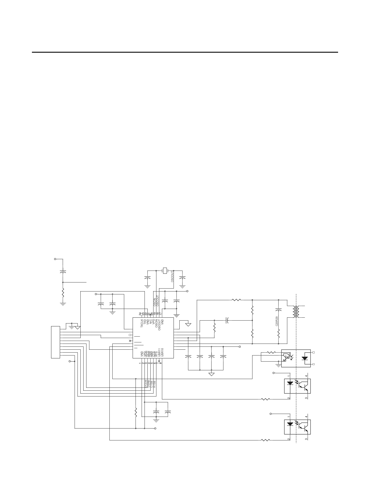
RECOMMENDED SCHEMATIC ARRANGEMENT
VCC3_3D
+ C1
10uF
RST
R1
10K
TXDB
VCC3_3D
J1
CON10
10
9
8
7
6
5
4
3
2
1
RXDB
DTRB
TXDB
RIB
DCDB
DSRB
CTSB
RTSB
VCC3_3
VCC3_3A
TXDB
C11 + C12
0.1uF 10uF
U1
25
RXDB 26
27
DTRB 28
29
30
HOOKB 31
RIB 32
VPD
RXD
RXCLK
DTR
USR20
RING
RELAY
RI
DCDB
DSRB
CTSB
RTSB
11.0592 MHz
C2
Y1
27pF
C3
33pF
C13
+
VCC3_3D
C14
R17
475
TXAP
ISOLATION BARRIER
T1P3
T1
10uF 0.1uF
C20
RXA 0.1uF
R15
5.1K
RXA_TAP
C4
.082UF
3
2
4
1
671-8005
VNA
RXA
VBG
VREF
TXAP
TXAN
VPA
RESET
16
15 RXA
14 VBG
13 VREF
12 TXAP
11
10
9 RST
C7
R23 NC
TXAN
C8 + C9
C10
R13
R2
21K
2K
VCC3_3A
TXAN
R28 120K
6
5
U2
1
2901CL_TQFP32 0.1uF 0.1uF 22uF 0.1uF
4
2
RINGB/PPUB/LIUB/LREVB
VCC3_3D
LDA110*
LIUCHECKB
R18
100
U10P2
U3
TLP627
R20
C5 +
C6
22K
10uF
0.1uF
VCC3_3D
VCC3_3
VCC3_3D
11
R16
100
HOOKB
U11P2
U4
TLP627
[js1]
Share Link: 