GS8180Q36D-100 Просмотр технического описания (PDF) - Giga Semiconductor
Номер в каталоге
Компоненты Описание
производитель
GS8180Q36D-100 Datasheet PDF : 32 Pages
| |||
GS8180Q18/36D-200/167/133/100*
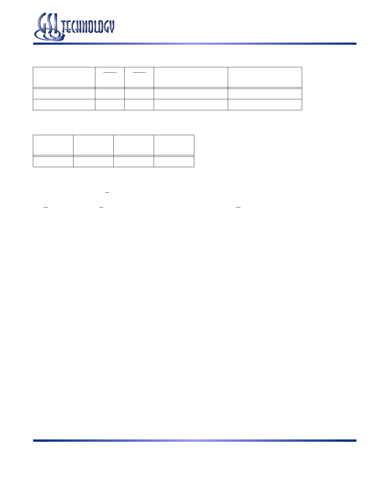
Example x18 RAM Write Sequence using Byte Write Enables
Data In Sample
Time
Beat 1
Beat 2
BW0 BW1
0
1
1
0
D0–D8
Data In
Don’t Care
D9–D17
Don’t Care
Data In
Resulting Write Operation
Beat 1
D0–D8
Written
Beat 1
D9–D17
Unchanged
Beat 2
D0–D8
Unchanged
Beat 2
D9–D17
Written
Output Register Control
SigmaQuad SRAMs offer two mechanisms for controlling the output data registers. Typically, control is handled by the Output
Register Clock inputs, C and C. The Output Register Clock inputs can be used to make small phase adjustments in the firing of the
output registers by allowing the user to delay driving data out as much as a few nanoseconds beyond the next rising edges of the K
and K clocks. If the C and C clock inputs are tied high, the RAM reverts to K and K control of the outputs, allowing the RAM to
function as a conventional pipelined read SRAM.
Rev: 2.03 10/2004
7/32
Specifications cited are subject to change without notice. For latest documentation see http://www.gsitechnology.com.
© 2002, GSI Technology
Share Link: 