GS8180Q36D-200 Просмотр технического описания (PDF) - Giga Semiconductor
Номер в каталоге
Компоненты Описание
производитель
GS8180Q36D-200 Datasheet PDF : 32 Pages
| |||
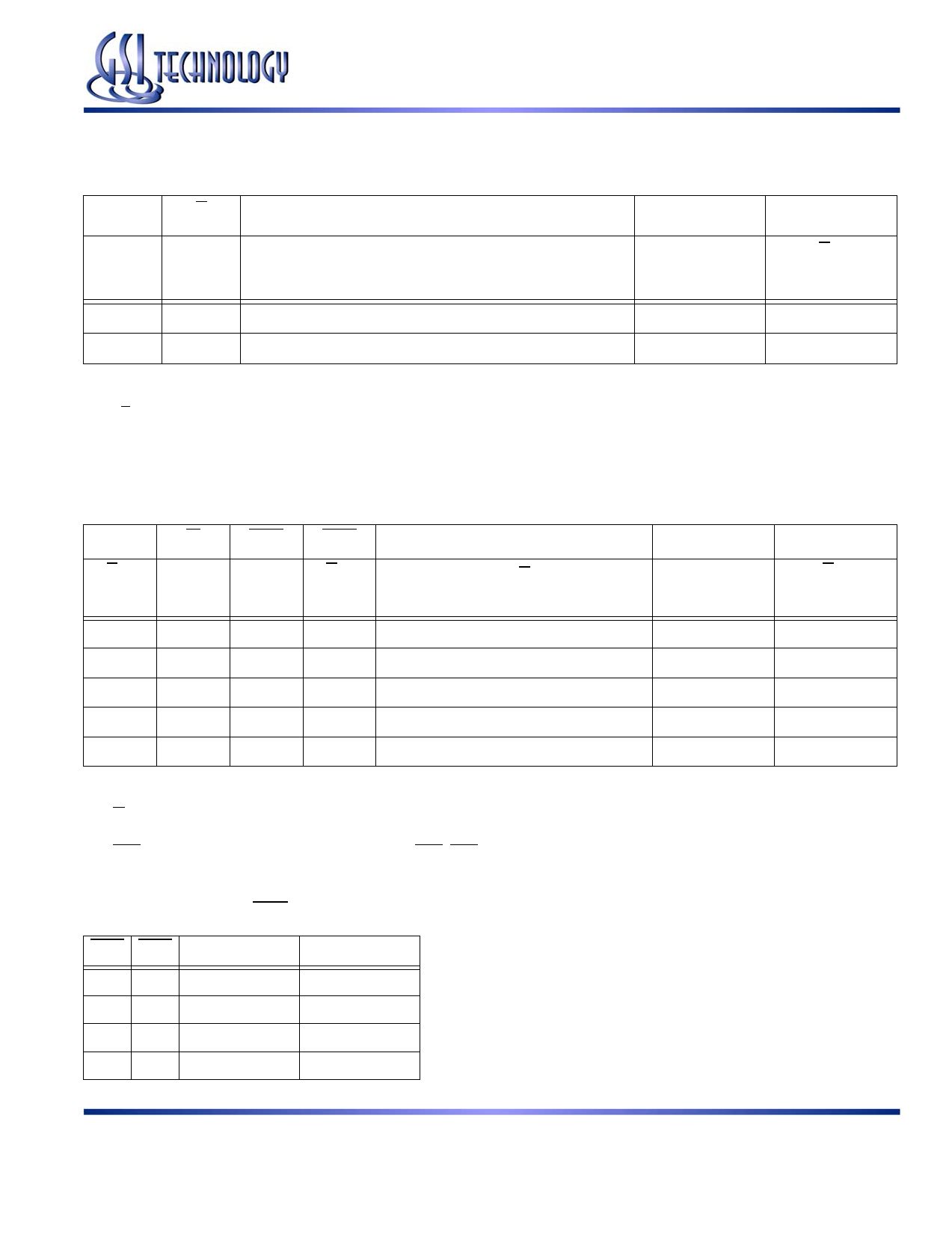
GS8180Q18/36D-200/167/133/100*
Separate I/O Burst of 2 SigmaQuad SRAM Read Truth Table
A
R
Output Next State
K↑
K↑
K↑
(tn)
(tn)
(tn)
X
1
Deselect
V
0
Read
Notes:
1. X = Don’t Care, 1 = High, 0 = Low, V = Valid.
2. R is evaluated on the rising edge of K.
3. Q0 and Q1 are the first and second data output transfers in a read.
Q
K↑
(tn+1)
Hi-Z
Q0
Separate I/O Burst of 2 SigmaQuad SRAM Write Truth Table
A
W
BWn BWn
Input Next State
D
K↑ K↑ K↑ K↑
K ↑, K ↑
K↑
(tn + ½) (tn)
(tn) (tn + ½)
(tn), (tn + ½)
(tn)
V
0
0
0
Write Byte Dx0, Write Byte Dx1
D0
V
0
0
1
Write Byte Dx0, Write Abort Byte Dx1
D0
V
0
1
0
Write Abort Byte Dx0, Write Byte Dx1
X
X
0
1
1
Write Abort Byte Dx0, Write Abort Byte Dx1
X
X
1
X
X
Deselect
X
Notes:
1. X = Don’t Care, H = High, L = Low, V = Valid.
2. W is evaluated on the rising edge of K.
3. D0 and D1 are the first and second data input transfers in a write.
4. BWn represents any of the Byte Write Enable inputs (BW0, BW1, etc.).
x18 Byte Write Enable (BWn) Truth Table
BW0 BW1
1
1
0
1
1
0
0
0
D0–D8
Don’t Care
Data In
Don’t Care
Data In
D9–D17
Don’t Care
Don’t Care
Data In
Data In
Q
K↑
(tn+1½)
Hi-Z
Q1
D
K↑
(tn + ½)
D1
X
D1
X
X
Rev: 2.03 10/2004
11/32
Specifications cited are subject to change without notice. For latest documentation see http://www.gsitechnology.com.
© 2002, GSI Technology
Share Link: 