GS8180Q18D-300(2002) Просмотр технического описания (PDF) - Giga Semiconductor
Номер в каталоге
Компоненты Описание
производитель
GS8180Q18D-300 Datasheet PDF : 29 Pages
| |||
Preliminary
GS8180Q18/36D-200/167/133
Special Functions
Byte Write Control
Byte Write Enable pins are sampled at the same time that Data In is sampled. A high on the Byte Write Enable pin associated with a particular
byte (e.g., BW0 controls D0–D8 inputs) will inhibit the storage of that particular byte, leaving whatever data may be stored at the current address
at that byte location undisturbed. Any or all of the Byte Write Enable pins may be driven high or low during the data in sample times in a write
sequence.
Each write enable command and write address loaded into the RAM provides the base address for a 2 beat data transfer. The x18 version of the
RAM, for example, may write 36 bits in association with each address loaded. Any 9-bit byte may be masked in any write sequence.
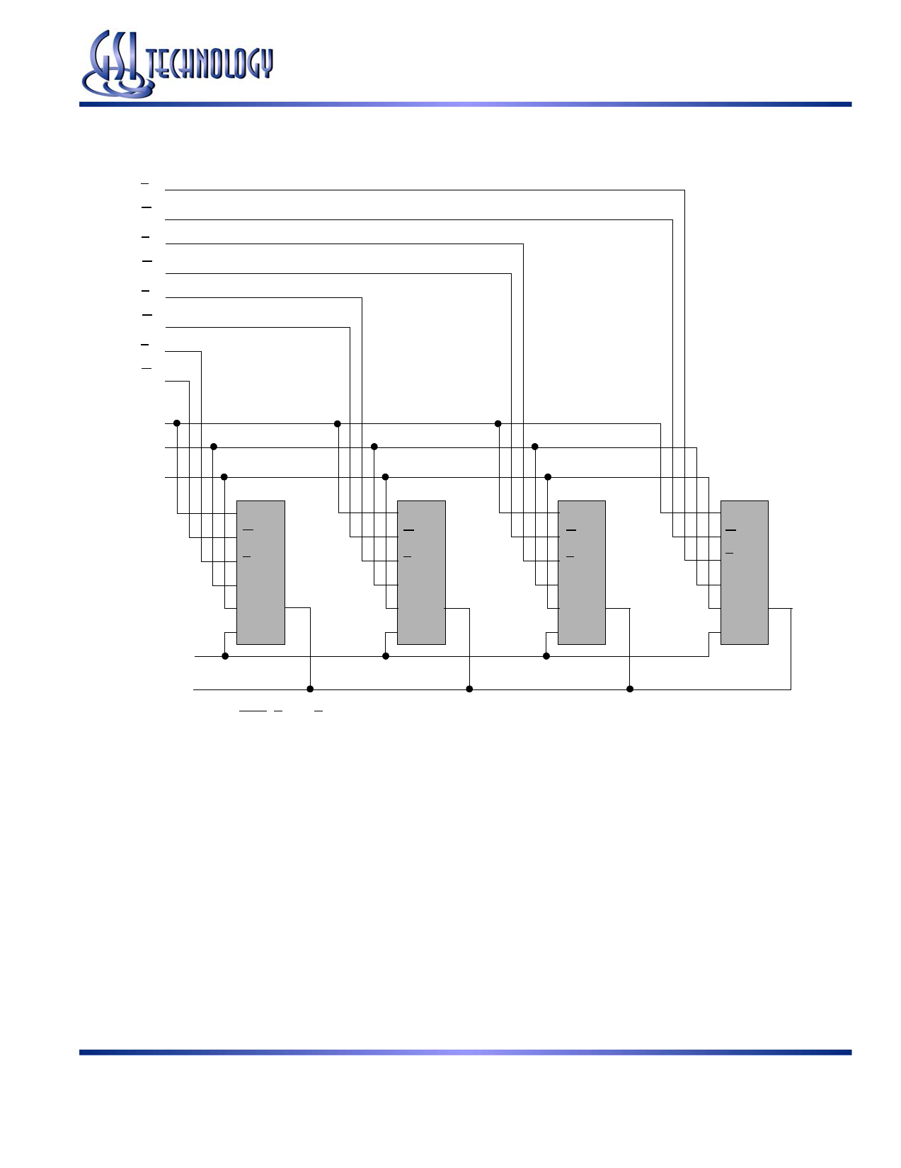
Example x18 RAM Write Sequence using Byte Write Enables
Data In Sample
Time
BW0 BW1
D0–D8
Beat 1
0
1
Data In
Beat 2
1
0
Don’t Care
D9–D17
Don’t Care
Data In
Resulting Write Operation
Byte 1
D0–D8
Byte 2
D9–D17
Written
Unchanged
Byte 3
D0–D8
Unchanged
Byte 4
D9–D17
Written
Output Register Control
SigmaQuad SRAMs offer two mechanisms for controlling the output data registers. Typically, control is handled by the Output Register Clock
inputs, C and C. The Output Register Clock inputs can be used to make small phase adjustments in the firing of the output registers by allowing
the user to delay driving data out as much as a few nanoseconds beyond the next rising edges of the K and K clocks. If the C and C clock inputs
are tied high, the RAM reverts to K and K control of the outputs, allowing the RAM to function as a conventional pipelined read SRAM.
Echo Clock
SigmaQuad SRAMs feature Echo Clock outputs, CQ and CQ, that track the performance of the output drivers. The Echo Clocks are delayed
copies of the Output Register clocks, C and C or K and K (if the C and C clock inputs are tied high). Echo Clocks are designed to track changes
in output driver delays due to variance in die temperature and supply voltage. The Echo Clocks are designed to fire with the rest of the data
output drivers. SigmaQuad SRAMs provide both in-phase, or true, Echo Clock output, CQ and inverted Echo Clock output CQ.
Echo Clocks are always active. Neither inhibiting reads via holding R high, nor deselection of the RAM via holding R and W high will
deactivate the Echo Clocks.
Rev: 2.00f 6/2002
8/29
© 2002, Giga Semiconductor, Inc.
Specifications cited are design targets and are subject to change without notice. For latest documentation contact your GSI representative.
Share Link: 