GS8180Q18D-333(2002) Просмотр технического описания (PDF) - Giga Semiconductor
Номер в каталоге
Компоненты Описание
производитель
GS8180Q18D-333 Datasheet PDF : 29 Pages
| |||
Preliminary
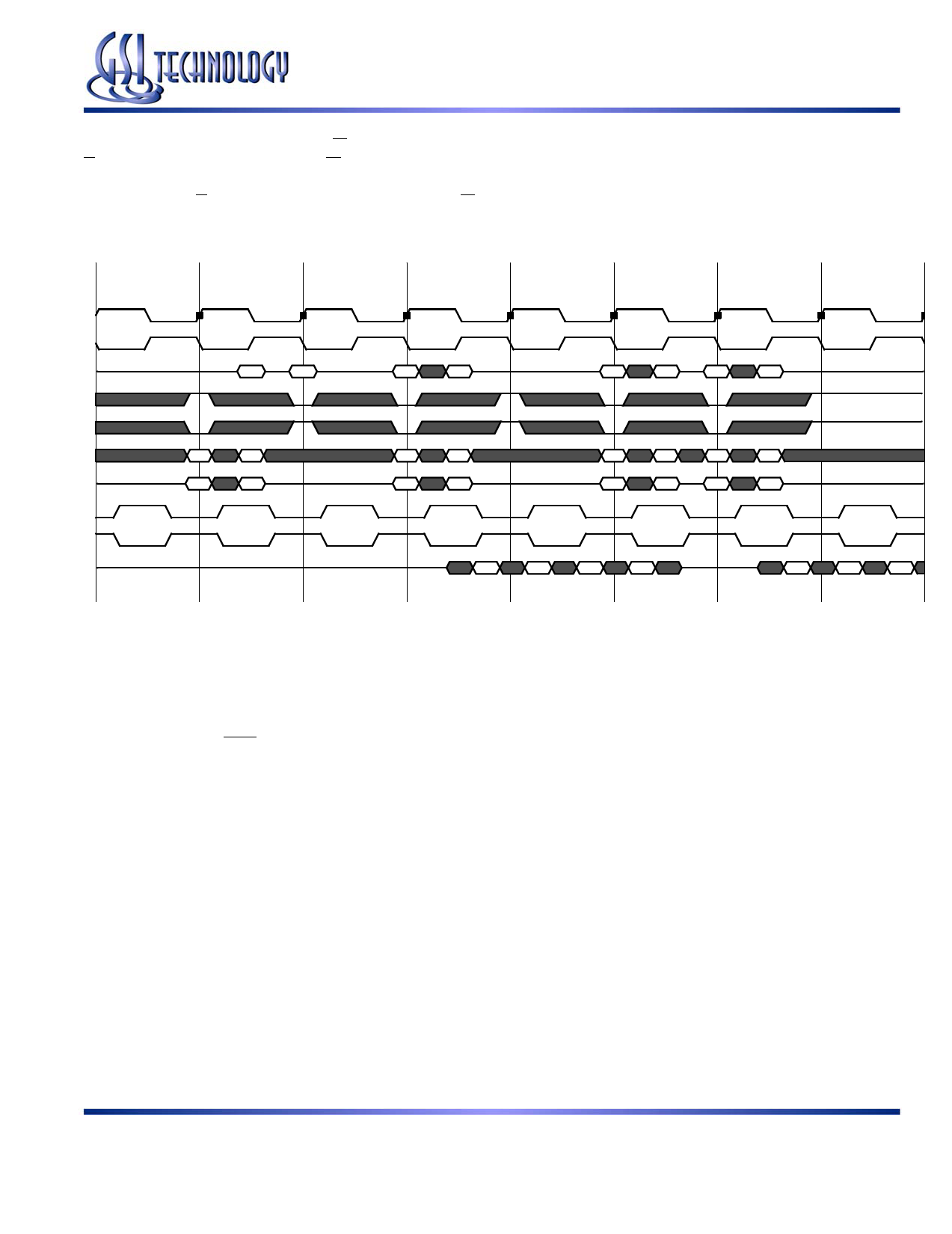
GS8180Q18/36D-200/167/133
Σ2x2B2 SigmaQuad SRAM DDR Read
The read port samples the status of the Address Input and R pins at each rising edge of K. A low on the Read Enable-bar pin, R, begins a read
cycle. Data can be clocked out one cycle later and again one half cycle after that. A high on the Read Enable-bar pin, R, begins a read port
deselect cycle.
Σ2x2B2 Double Data Rate SigmaQuad SRAM Read First
Dwg Rev. G
No Op
No Op
Read
Write
Read
Write
Read
Write
K
/K
Address
XX
XX
B
C
D
E
F
G
/R
/W
/BWx
DC0
DC1
DE0
DE1
DG0
DG1
D
C
/C
Q
QB0
QB1
CQ
/CQ
Rev: 2.00f 6/2002
6/29
© 2002, Giga Semiconductor, Inc.
Specifications cited are design targets and are subject to change without notice. For latest documentation contact your GSI representative.
Share Link: 