GS8180Q36D-133(2002) Просмотр технического описания (PDF) - Giga Semiconductor
Номер в каталоге
Компоненты Описание
производитель
GS8180Q36D-133 Datasheet PDF : 29 Pages
| |||
Preliminary
GS8180Q18/36D-200/167/133
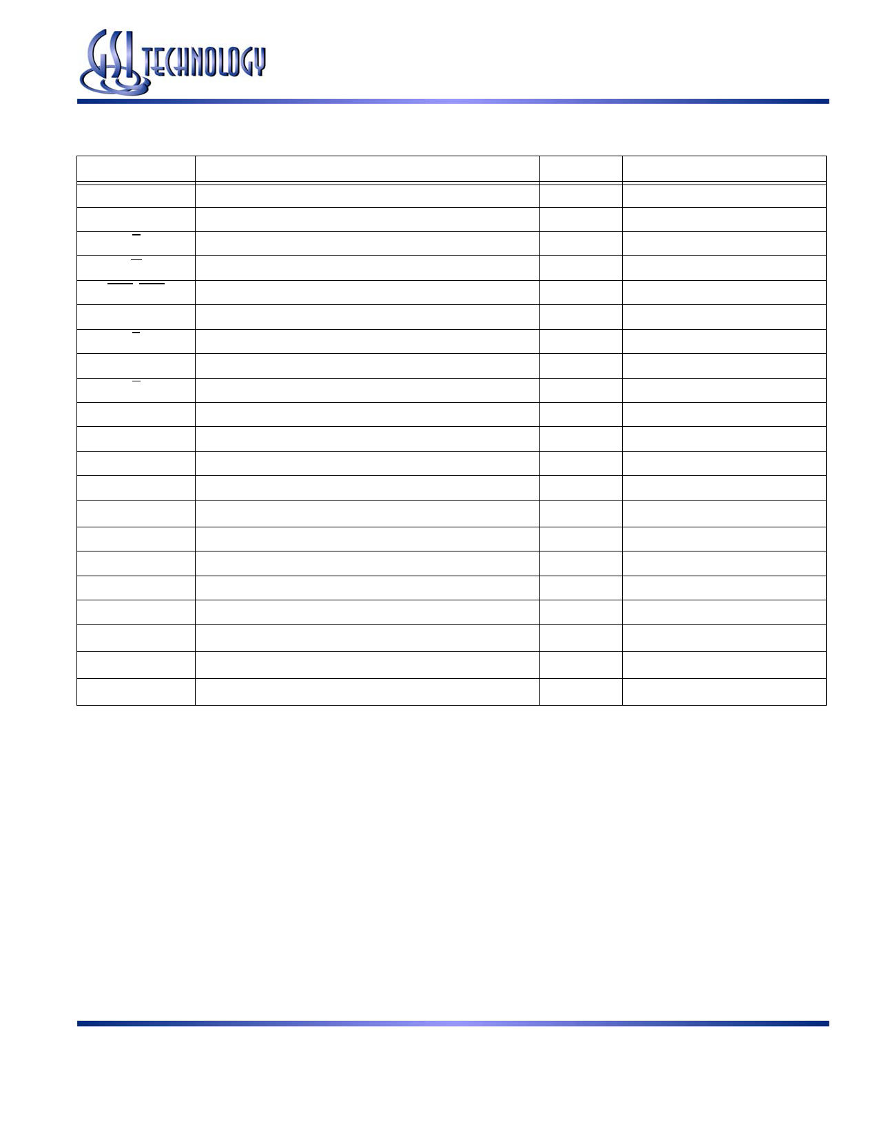
Pin Description Table
Pin Location
Symbol
Description
Type Comments
B4, B8, C5, C6, C7, N5, N6, N7, P4, P5 P7, P8, R3, R4,
R5, R7, R8, R9
SA
Synchronous Address Inputs
Input
—
A9
SA
Synchronous Address Inputs
Input
x18 Version
A9
NC
No Connect
—
x36 Version
A8
R
Synchronous Read
Input
Active Low
A4
W
Synchronous Write
Input
Active Low
B7, A5
BW0–BW1
Synchronous Byte Writes
Input
Active Low
x18 Version
A7, B5
NC
No Connect
—
x18 Version
B7, A7, A5, B5
BW0–BW3
Synchronous Byte Writes
Input
Active Low
x36 Version
B6
K
Input Clock
Input
Active High
A6
K
Input Clock
Input
Active Low
P6
C
Output Clock
Input
Active High
R6
C
Output Clock
Input
Active Low
R10
TMS
Test Mode Select
Input
—
R11
TDI
Test Data Input
Input
—
R2
TCK
Test Clock Input
Input
—
R1
TDO
Test Data Output
Output
—
H2, H10
VREF
HSTL Input Reference Voltage Input
—
H11
ZQ
Output Impedance Matching Input Input
—
A2, A10
MCL
Must Connect Low
—
—
A11
CQ
Synchronous Echo Clock Output Output Echoes C or K Clock
A1
CQ Synchronous Echo Clock-bar Output Output Echoes C or K Clock
B1, B2, B10, B11, C2, C10, D3, D9, E1, E3, E9, E11, F1,
F2, F10, F11, G3, G9, J2, J10, K1, K3, K9,K11, L1, L2,
L10, L11, M2, M10, N3, N9, P1, P3, P9, P11
Q0–Q35
Synchronous Data Outputs
Output
x36 Version
B3, C3, C11, D2, D11, E10, F3, G2, G11, J3, J11, K10,
L3, M3, M11, N2, N11, P10
D0–D17
Synchronous Data Inputs
Input
x18 Version
B2, B11, C10, D3, E3, E11, F2, F11, G3, J10, K3, K11,
L2, L11, M10, N3, P3, P11
Q0–Q17
Synchronous Data Outputs
Output
x18 Version
B1, B9, B10, C1, C2, C9, D1, D9, D10, E1, E2, E9, F1,
F9, F10, G1, G9, G10, J1, J2, J9, K1, K2, K9, L1, L9, L10, NC
M1, M2, M9, N1, N9, N10, P1, P2, P9
No Connect
—
x18 Version
A3, H1
NC
No Connect
—
F5, F7, G5, G7, H5, H7, J5, J7, K5, K7
VDD
Power Supply
Supply 1.8 V Nominal
Rev: 2.00f 6/2002
4/29
© 2002, Giga Semiconductor, Inc.
Specifications cited are design targets and are subject to change without notice. For latest documentation contact your GSI representative.
Share Link: 