TQ6122-M Просмотр технического описания (PDF) - TriQuint Semiconductor
Номер в каталоге
Компоненты Описание
производитель
TQ6122-M Datasheet PDF : 23 Pages
| |||
TQ6122
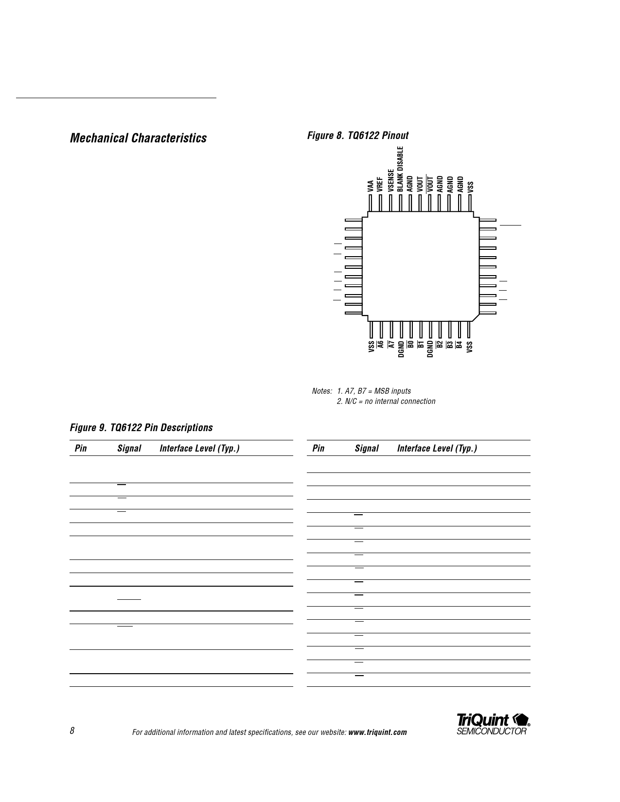
Mechanical Characteristics
Figure 8. TQ6122 Pinout
The TQ6122 DAC is packaged in a proprietary 44-pin
multilayer ceramic package which provides high-speed,
controlled-impedance interconnects and integral power
supply bypassing. The leads are set on 0.050” centers,
and are formed for gull-wing surface mounting. Figure
8 shows the pinout diagram of the packaged IC as seen
from the top, opposite the cavity side; Figure 9 lists pin
numbers, names and I/O levels. Figure 10 illustrates
the pertinent dimensions of the package and Figure 11
shows the mounting footprint.
Since the TQ6122 dissipates on the order of 1.3 W,
adequate heat sinking is essential for proper operation
of the device. Figure 12 shows one possible heat sink
arrangement based on a multi-finned “Top Hat” heat
sink available from Thermalloy. An environment with a
minimum of 100 fpm (feet per minute) of forced air
cooling is assumed; >200 fpm is preferred.
VAA
IREF
ECL REF
A0
A1
DGND
A2
A3
A4
A5
VSS
12
23
11
TQ6122AM
TOP VIEW
OF MLC-44 PACKAGE
AS IT SITS ON
CIRCUIT BOARD
(CAVITY IS DOWN)
34
PIN 1
Notes: 1. A7, B7 = MSB inputs
2. N/C = no internal connection
VSS
CLOCK
CLOCK
N/C
SELA
DGND
BLANK
B7
B6
B5
VSS
Figure 9. TQ6122 Pin Descriptions
Pin
Signal Interface Level (Typ.)
1, 11, 12,
33, 34, 44
2
3
4
5
6, 28,
37, 40
7
8
9
10
13–15, 18
16
17
19
20
VSS
B5
B6
B7 (MSB)
BLANK
DGND
SELA
—
CLOCK
CLOCK
AGND
VOUT
VOUT
BLANK
DISABLE
VSENSE
–5 V
600 mV pk–pk centered at –1.3 V @ DC
600 mV pk–pk centered at –1.3 V @ DC
600 mV pk–pk centered at –1.3 V @ DC
600 mV pk–pk centered at –1.3 V @ DC
0V
600 mV pk–pk centered at –1.3 V @ DC
No connection
1V pk–pk centered at –1.3 V @ AC
1V pk–pk centered at –1.3 V @ AC
0V
0 V to –1 V
–1 V to 0 V
Enable = VAA (IBLANK = ON)
Disable = AGND (IBLANK = OFF)
VAA + 0.8, for VFS = 1 V pk–pk
Pin
21
22, 23
24
25
26
27
29
30
31
32
35
36
38
39
41
42
43
Signal Interface Level (Typ.)
VREF
VAA
IREF
ECL REF
A0 (LSB)
A1
A2
A3
A4
A5
A6
A7 (MSB)
B0 (LSB)
B1
B2
B3
B4
VAA +1, for VFS = 1V pk–pk
–5 V
2.5 mA for VFS = 1V pk–pk
–1.3 V
600 mV pk–pk centered at –1.3 V @ DC
600 mV pk–pk centered at –1.3 V @ DC
600 mV pk–pk centered at –1.3 V @ DC
600 mV pk–pk centered at –1.3 V @ DC
600 mV pk–pk centered at –1.3 V @ DC
600 mV pk–pk centered at –1.3 V @ DC
600 mV pk–pk centered at –1.3 V @ DC
600 mV pk–pk centered at –1.3 V @ DC
600 mV pk–pk centered at –1.3 V @ DC
600 mV pk–pk centered at –1.3 V @ DC
600 mV pk–pk centered at –1.3 V @ DC
600 mV pk–pk centered at –1.3 V @ DC
600 mV pk–pk centered at –1.3 V @ DC
8
For additional information and latest specifications, see our website: www.triquint.com
Share Link: 