2SK3453 Просмотр технического описания (PDF) - Toshiba
Номер в каталоге
Компоненты Описание
производитель
2SK3453 Datasheet PDF : 6 Pages
| |||
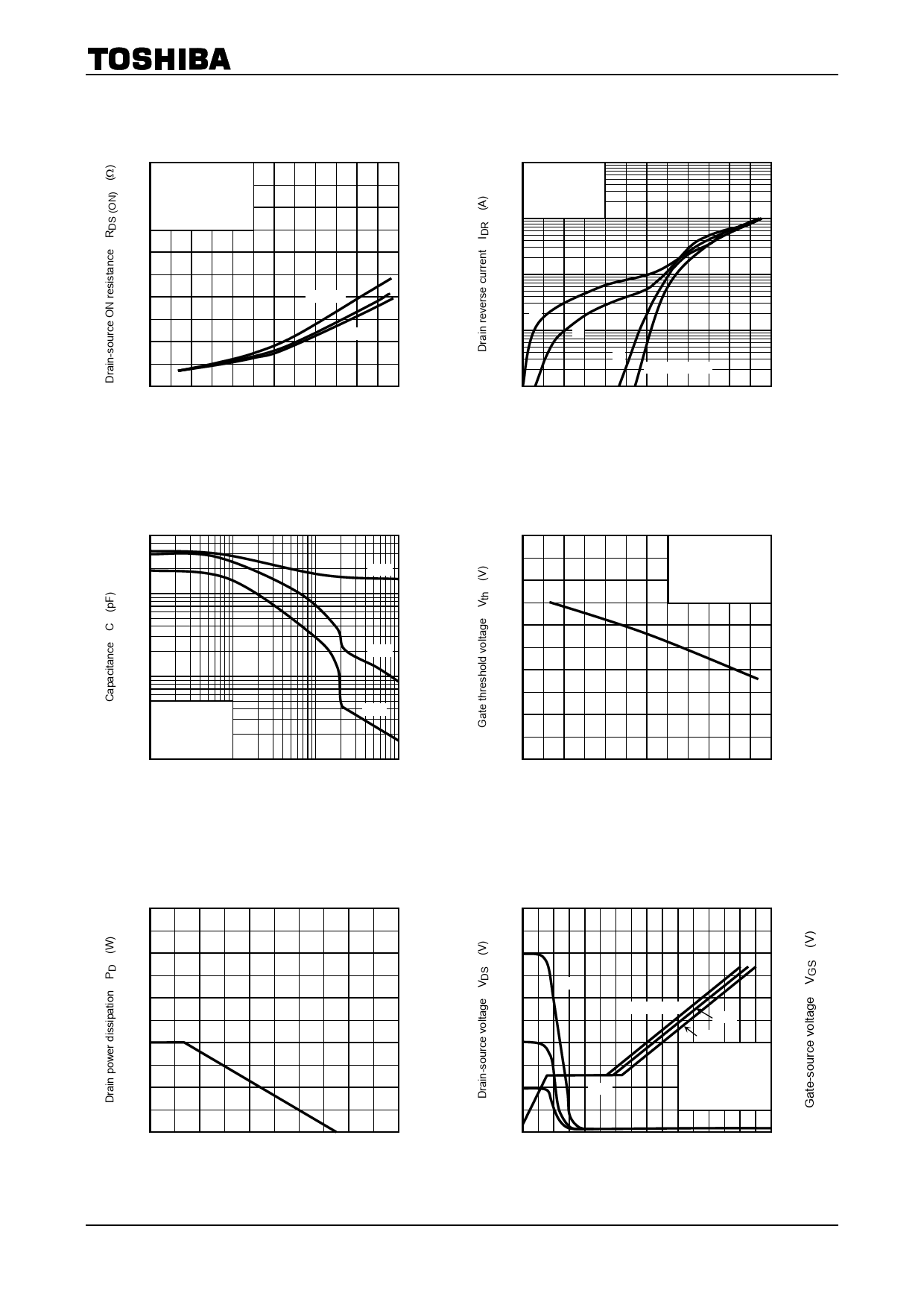
RDS (ON) − Tc
10
Common source
VGS = 10 V
8 Pulse test
6
5
4
ID = 10 A
2.5
2
0
−80
−40
0
40
80
120
160
Case temperature Tc (°C)
2SK3453
100
50 Common source
30 Tc = 25°C
Pulse test
10
5
3
IDR − VDS
1
0.5
0.3
10
0.1
3
0.05
0.03
1
VGS = 0, −1 V
0.01
0
−0.2 −0.4 −0.6 −0.8 −1.0 −1.2
Drain-source voltage VDS (V)
Capacitance – VDS
5000
3000
Ciss
1000
500
300
Coss
100
50
Common source
30 VGS = 0 V
f = 1 MHz
Tc = 25°C
10
0.1
0.3 0.5 1
Crss
3 5 10
30 50 100
Drain-source voltage VDS (V)
Vth − Tc
5
Common source
VDS = 10 V
ID = 1 mA
4
Pulse test
3
2
1
0
−80
−40
0
40
80
120
160
Cace temperature Tc (°C)
PD − Tc
200
160
120
80
40
10
0
40
80
120
160
200
Case temperature Tc (°C)
Dynamic input/output characteristics
500
20
400
16
VDS
300
12
VDS = 100 V
200
200
100
VGS
400
8
Common source
ID = 10 A
Tc = 25°C
Pulse test
4
0
0
0 10 20 30 40 50 60 70 80
Total gate charge Qg (nC)
4
2009-09-29
Share Link: 