2SK2956-E Просмотр технического описания (PDF) - Renesas Electronics
Номер в каталоге
Компоненты Описание
производитель
2SK2956-E Datasheet PDF : 7 Pages
| |||
2SK2956
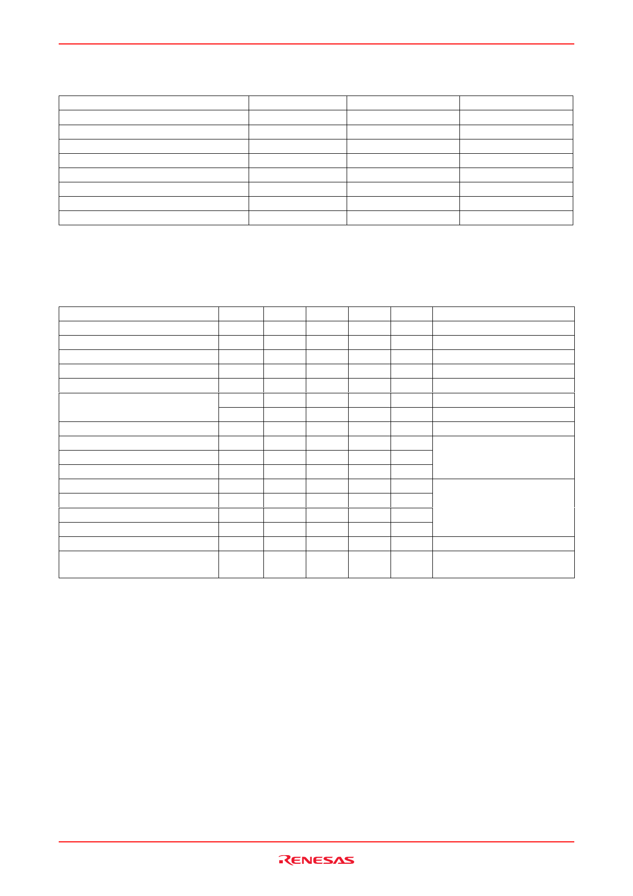
Absolute Maximum Ratings
Item
Drain to source voltage
Gate to source voltage
Drain current
Drain peak current
Body-drain diode reverse drain current
Channel dissipation
Channel temperature
Storage temperature
Notes: 1. PW ≤ 10 µs, duty cycle ≤ 1 %
2. Value at Tc = 25°C
Symbol
VDSS
VGSS
ID
ID(pulse)Note1
IDR
Pch Note2
Tch
Tstg
Ratings
30
±20
50
200
50
35
150
–55 to +150
(Ta = 25°C)
Unit
V
V
A
A
A
W
°C
°C
Electrical Characteristics
Item
Symbol Min
Drain to source breakdown voltage V(BR)DSS 30
Gate to source breakdown voltage V(BR)GSS ±20
Zero gate voltage drain current
IDSS
—
Gate to source leak current
IGSS
—
Gate to source cutoff voltage
VGS(off)
1.0
Static drain to source on state
resistance
RDS(on)
—
RDS(on)
—
Forward transfer admittance
|yfs|
25
Input capacitance
Ciss
—
Output capacitance
Coss
—
Reverse transfer capacitance
Crss
—
Turn-on delay time
td(on)
—
Rise time
tr
—
Turn-off delay time
td(off)
—
Fall time
tf
—
Body–drain diode forward voltage
VDF
—
Body–drain diode reverse
recovery time
trr
—
Note: 3. Pulse test
Typ
—
—
—
—
—
7.0
12
45
2000
1500
350
20
330
190
190
0.95
60
Max
—
—
10
±10
2.0
10
18
—
—
—
—
—
—
—
—
—
—
Unit
V
V
µA
µA
V
mΩ
mΩ
S
pF
pF
pF
ns
ns
ns
ns
V
ns
(Ta = 25°C)
Test Conditions
ID = 10 mA, VGS = 0
IG = ±100 µA, VDS = 0
VDS = 30 V, VGS = 0
VGS = ±16 V, VDS = 0
ID = 1 mA, VDS = 10V
ID = 25 A, VGS = 10V Note3
ID = 25 A, VGS = 4V Note3
ID = 25 A, VDS = 10V Note3
VDS = 10 V, VGS = 0,
f = 1MHz
VGS = 10 V, ID = 25 A,
RL = 0.4 Ω
IF = 50 A, VGS = 0
IF = 50 A, VGS = 0
diF/ dt = 50 A/ µs
Rev.4.01 Apr 27, 2006 page 2 of 6
Share Link: 