J506 Просмотр технического описания (PDF) - Renesas Electronics
Номер в каталоге
Компоненты Описание
производитель
J506 Datasheet PDF : 8 Pages
| |||
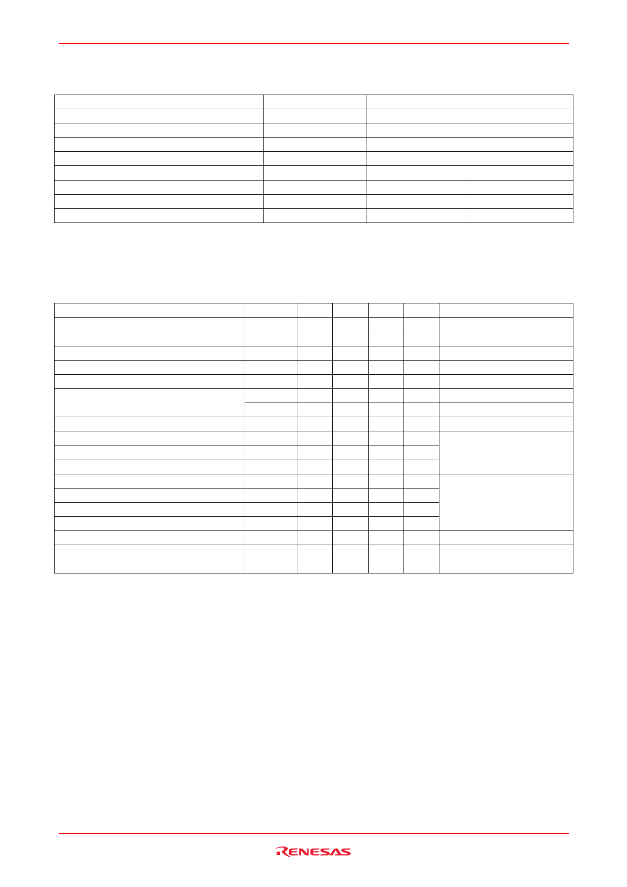
2SJ506(L), 2SJ506(S)
Absolute Maximum Ratings
Item
Drain to source voltage
Gate to source voltage
Drain current
Drain peak current
Body to drain diode reverse drain current
Channel dissipation
Channel temperature
Storage temperature
Notes: 1. PW ≤ 10 µs, duty cycle ≤ 1%
2. Value at Tc = 25°C
Symbol
VDSS
VGSS
ID
ID (pulse) Note 1
IDR
Pch Note 2
Tch
Tstg
Value
–30
±20
–10
–40
–10
20
150
–55 to +150
(Ta = 25°C)
Unit
V
V
A
A
A
W
°C
°C
Electrical Characteristics
Item
Drain to source breakdown voltage
Gate to source breakdown voltage
Zero gate voltage drain current
Gate to source leak current
Gate to source cutoff voltage
Static drain to source on state resistance
Forward transfer admittance
Input capacitance
Output capacitance
Reverse transfer capacitance
Turn-on delay time
Rise time
Turn-off delay time
Fall time
Body to drain diode forward voltage
Body to drain diode reverse recovery time
Note: 3. Pulse test
Symbol
V (BR) DSS
V (BR) GSS
IDSS
IGSS
VGS (off)
RDS (on)
RDS (on)
|yfs|
Ciss
Coss
Crss
td (on)
tr
td (off)
tf
VDF
trr
Min Typ Max
–30 —
—
±20 —
—
—
— –10
—
— ±10
–1.0 — –2.0
—
65
85
— 110 180
10
16
—
— 660 —
— 440 —
— 140 —
—
12
—
—
65
—
—
85
—
—
65
—
— –1.05 —
—
65
—
Unit
V
V
µA
µA
V
mΩ
mΩ
S
pF
pF
pF
ns
ns
ns
ns
V
ns
(Ta = 25°C)
Test Conditions
ID = –10 mA, VGS = 0
IG = ±100 µA, VDS = 0
VDS = –30 V, VGS = 0
VGS = ±16 V, VDS = 0
ID = –1 mA, VDS = –10 V
ID = –5 A, VGS = –10 V Note 3
ID = –5 A, VGS = –4 V Note 3
ID = –5 A, VDS = –10 V Note 3
VDS = –10 V
VGS = 0
f = 1 MHz
VGS = –10 V
ID = –5 A
RL = 2 Ω
IF = –10 A, VGS = 0
IF = –10 A, VGS = 0
diF/dt = 50 A/µs
Rev.5.00 Sep 07, 2005 page 2 of 7
Share Link: 