V62C31864 Просмотр технического описания (PDF) - Mosel Vitelic Corporation
Номер в каталоге
Компоненты Описание
производитель
V62C31864 Datasheet PDF : 12 Pages
| |||
MOSEL VITELIC
Pin Descriptions
A0–A12 Address Inputs
These 13 address inputs select one of the 8,192 x 8
bit segments in the RAM.
CE1, CE2 Chip Enable Inputs
CE1 is active LOW and CE2 is active HIGH. Both
chip enables must be active to read from or write to
the device. If either chip enable is not active, the
device is deselected and is in a standby power
mode. The I/O pins will be in the high-impedance
state when deselected.
OE
Output Enable Input
The Output Enable input is active LOW. When OE
is LOW with CE1 LOW, CE2 HIGH, and WE HIGH,
data of the selected memory location will be
available on the I/O pins. When OE is HIGH, the I/O
pins will be in the high impedance state.
V62C31864
WE
Write Enable Input
An active LOW input, WE input controls read and
write operations. When CE1 and WE inputs are
both LOW with CE2 HIGH, the data present on the
I/O pins will be written into the selected memory
location.
I/O0–I/O7 Data Input and Data Output Ports
These 8 bidirectional ports are used to read data
from and write data into the RAM.
VCC
GND
Power Supply
Ground
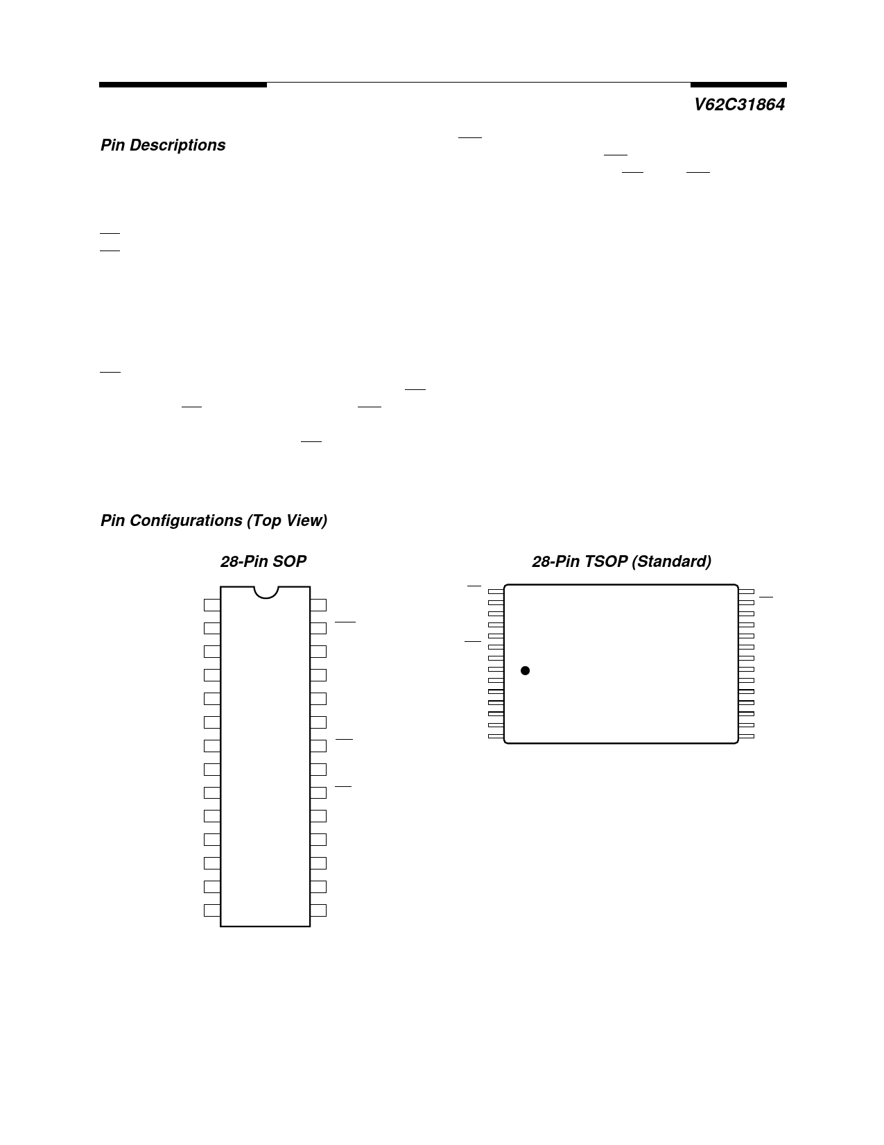
Pin Configurations (Top View)
28-Pin SOP
NC 1
A12
2
A7
3
A6
4
A5
5
A4
6
A3
7
A2
8
A1
9
A0
10
I/O0
11
I/O1
12
I/O2
13
GND 14
28
27
26
25
24
23
22
21
20
19
18
17
16
15
51864 02
VCC
WE
CE2
A8
A9
A11
OE
A10
CE1
I/O7
I/O6
I/O5
I/O4
I/O3
OE
A11
A9
A8
CE2
WE
VCC
NC
A12
A7
A6
A5
A4
A3
28-Pin TSOP (Standard)
22
21
A10
23
20
CE1
24
19
I/O7
25
18
I/O6
26
17
I/O5
27
16
I/O4
28
15
I/O3
1
14
GND
2
13
I/O2
3
12
I/O1
4
11
I/O0
5
10
A0
6
9
A1
7
8
A2
51864 03
V62C31864 Rev. 1.6 August 1998
2
Share Link: 