3055L Просмотр технического описания (PDF) - Intersil
Номер в каталоге
Компоненты Описание
производитель
3055L Datasheet PDF : 10 Pages
| |||
RFT3055LE
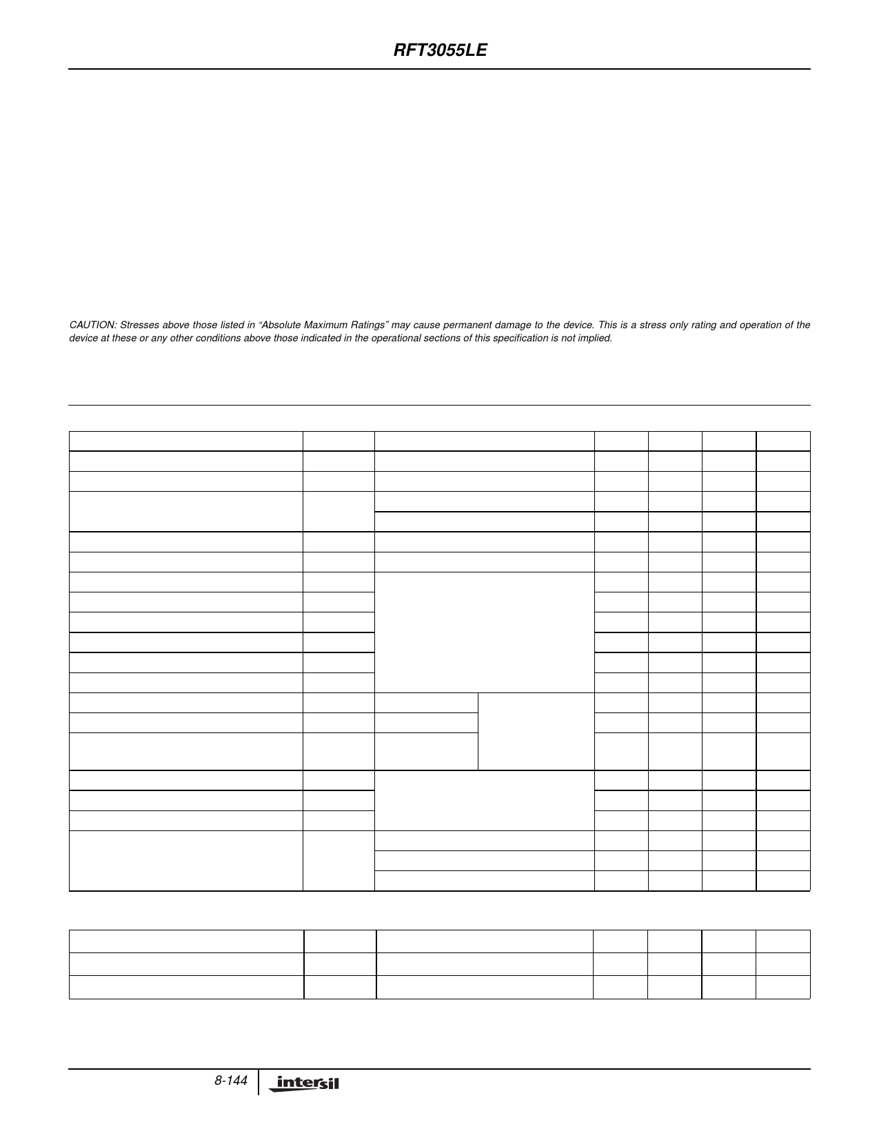
Absolute Maximum Ratings TA = 25oC, Unless Otherwise Specified
RFT3055LE
UNITS
Drain to Source Voltage (Note 1) . . . . . . . . . . . . . . . . . . . . . . . . . . . . . . . . . . . . . . . . . . VDSS
Drain to Gate Voltage (RGS = 20kΩ) (Note 1) . . . . . . . . . . . . . . . . . . . . . . . . . . . . . . . .VDGR
Gate to Source Voltage . . . . . . . . . . . . . . . . . . . . . . . . . . . . . . . . . . . . . . . . . . . . . . . . . . VGS
Drain Current
60
V
60
V
±10
V
Continuous (Figure 2) (Note 2). . . . . . . . . . . . . . . . . . . . . . . . . . . . . . . . . . . . . . . . . . . . . ID
Pulsed Drain Current . . . . . . . . . . . . . . . . . . . . . . . . . . . . . . . . . . . . . . . . . . . . . . . . . . IDM
Pulsed Avalanche Rating . . . . . . . . . . . . . . . . . . . . . . . . . . . . . . . . . . . . . . . . . . . . . . . . . EAS
Power Dissipation (Note 2) . . . . . . . . . . . . . . . . . . . . . . . . . . . . . . . . . . . . . . . . . . . . . . . . PD
Derate Above 25oC . . . . . . . . . . . . . . . . . . . . . . . . . . . . . . . . . . . . . . . . . . . . . . . . . . . . . .
Operating and Storage Temperature . . . . . . . . . . . . . . . . . . . . . . . . . . . . . . . . . . . . TJ, TSTG
Maximum Temperature for Soldering
Leads at 0.063in (1.6mm) from Case for 10s. . . . . . . . . . . . . . . . . . . . . . . . . . . . . . . . . TL
Package Body for 10s, See Techbrief 334 . . . . . . . . . . . . . . . . . . . . . . . . . . . . . . . . . . Tpkg
2.0
Figure 5
Figures 6, 16, 17
1.1
9.09
-55 to 150
300
260
A
W
mW/oC
oC
oC
oC
CAUTION: Stresses above those listed in “Absolute Maximum Ratings” may cause permanent damage to the device. This is a stress only rating and operation of the
device at these or any other conditions above those indicated in the operational sections of this specification is not implied.
NOTE:
1. TJ = 25oC to 125oC.
Electrical Specifications TA = 25oC, Unless Otherwise Specified
PARAMETER
SYMBOL
TEST CONDITIONS
Drain to Source Breakdown Voltage
Gate to Source Threshold Voltage
Zero Gate Voltage Drain Current
Gate to Source Leakage Current
Drain to Source On Resistance
Turn-On Time
Turn-On Delay Time
Rise Time
Turn-Off Delay Time
Fall Time
Turn-Off Time
Total Gate Charge
Gate Charge at 10V
Threshold Gate Charge
BVDSS
VGS(TH)
IDSS
IGSS
rDS(ON)
tON
td(ON)
tr
td(OFF)
tf
tOFF
Qg(TOT)
Qg(5)
Qg(TH)
ID = 250µA, VGS = 0V (Figure 11)
VGS = VDS, ID = 250µA (Figure 10)
VDS = 60V, VGS = 0V
VDS = 60V, VGS = 0V, TA = 150oC
VGS = ±10V
ID = 2.0A, VGS = 5V (Figure 9)
VDD = 30V, ID ≅ 2.0A,
RL = 15Ω, VGS = 5V,
RGS = 5Ω
(Figure 12)
VGS = 0V to 10V
VGS = 0V to 5V
VGS = 0V to 1V
VDD = 30V,
ID ≅ 2.0A,
RL = 15Ω
Ig(REF) = 1.0mA
(Figure 15)
Input Capacitance
Output Capacitance
Reverse Transfer Capacitance
Thermal Resistance Junction to Ambient
CISS
COSS
CRSS
RθJA
VDS = 25V, VGS = 0V,
f = 1MHz
(Figure 12)
Pad Area = 0.171 in2 (see note 2)
Pad Area = 0.068 in2
Pad Area = 0.026 in2
MIN
TYP
MAX UNITS
60
-
-
V
1
-
2
V
-
-
1
µA
-
-
50
µA
-
-
10
µA
-
0.110 0.150
Ω
-
-
120
ns
-
10
-
ns
-
70
-
ns
-
30
-
ns
-
25
-
ns
-
-
85
ns
-
28
35
nC
-
15
18
nC
-
1.0
1.2
nC
-
850
-
pF
-
170
-
pF
-
100
-
pF
-
-
110
oC/W
-
-
128
oC/W
-
-
147
oC/W
Source to Drain Diode Specifications
PARAMETER
SYMBOL
TEST CONDITIONS
Source to Drain Diode Voltage
VSD
ISD = 2.0A
Reverse Recovery Time
trr
ISD = 2.0A, dISD/dt = 100A/µs
NOTE:
2. 110 oC/W measured using FR-4 board with 0.171in2 footprint for 1000 seconds.
MIN
TYP
MAX UNITS
-
-
1.5
V
-
-
100
ns
8-144
Share Link: 