LB1669 Просмотр технического описания (PDF) - SANYO -> Panasonic
Номер в каталоге
Компоненты Описание
производитель
LB1669 Datasheet PDF : 5 Pages
| |||
LB1669, 1669M
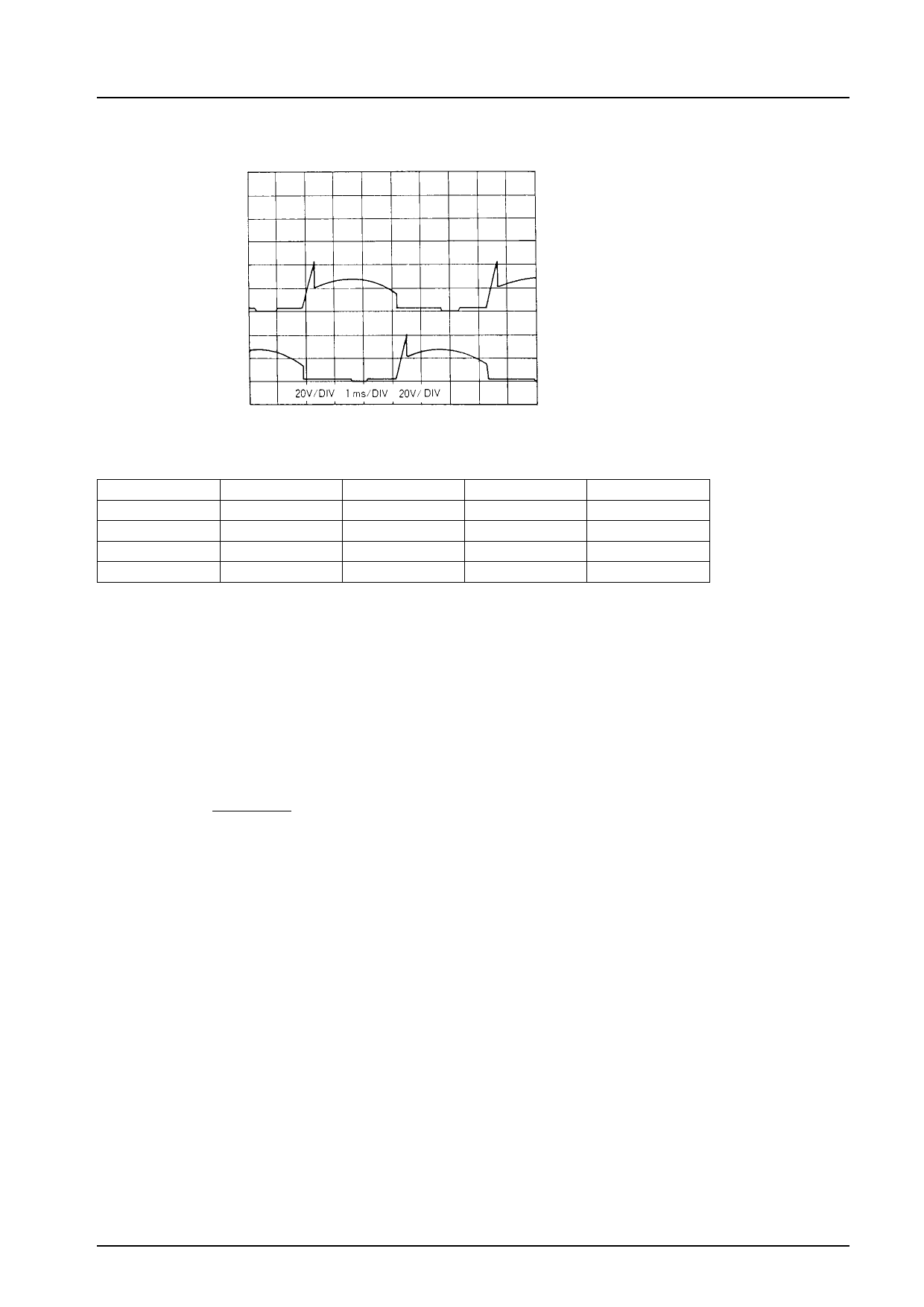
Sample Application Circuit 2 Output Waveform Diagram
Truth Table
IN+
IN–
H
L
L
H
H
L
L
H
C
OUT1
OUT2
L
H
L
L
L
H
H
H
H
H
H
H
Design Notes (See Sample Application Circuits.)
(1) Supply Voltage (VIN pin)
The LB1669 series have the internal parallel regulator which supplies power to the Hall amplifier circuit and the control
block. Therefore, the driver ICs are not affected by power source fluctuations and kickbacks from the motor. They maintain
the stable operations even if noise signals such as surge are generated.
Set the resistance R1 between VCC and VIN so that the ICC current of 6 mA to 50 mA can flow into the VIN pin within the
supply voltage range of a fan motor.
VIN is 6.7 V typ at ICC = 7 mA.
The current flowing into VIN is calculated using the equation shown below.
ICC = VCC – VIN . . . . . . . (1)
. R1
Consideration given to surge voltage
The maximum allowable current at VIN pin is 200 mA, so the withstand voltage level is designed as follows.
Vsurge = VIN + R1 × 200 mA . . . . . . (2)
(2) Hall input pin voltage (IN– and IN+ pins)
IN– and IN+ are input pins for the Hall element output. Set the Hall element output voltage to within the range of 0 V to VIN
– 1.5 V.
The gain between the Hall input pin and the output pin is 100 dB or greater. The offset voltage of the Hall input amplifier is
±7 mV therefore, the Hall element output must be set with the offset voltage (±7 mV) considered.
(3) Output transistors (OUT1 and OUT2 pins)
Output current IO = 1.5 A max.
Output saturation voltage VO sat = 1.15 V/1.0 A (typ.)
The LB1669 requires one of the three types of output protection.
1 When external capacitors are connected between OUT and GND, the capacitance should not exceed 10 µF. Use
capacitance that will hold kickback voltage and back voltage to 60 V or less.
2 When external Zener diodes are connected, use one that will have a cutoff voltage of 40 V or less. If radio noise is a
problem, insert a capacitor of 0.01 to 0.1µF between B1 and B2.
3 When external capacitors are connected between OUT and B, use one that will hold kickback voltage to 40 V or less.
If it oscillates, insert resistance in series with the capacitor.
No.3513-4/5
Share Link: 