MAX6720 –ü—Ä–æ—Å–º–æ—Ç—Ä —Ç–µ—Ö–Ω–∏—á–µ—Å–∫–æ–≥–æ –æ–ø–∏—Å–∞–Ω–∏—è (PDF) - Maxim Integrated
–ù–æ–º–µ—Ä –≤ –∫–∞—Ç–∞–ª–æ–≥–µ
–ö–æ–º–ø–æ–Ω–µ–Ω—Ç—ã –û–ø–∏—Å–∞–Ω–∏–µ
–ø—Ä–æ–∏–∑–≤–æ–¥–∏—Ç–µ–ª—å
MAX6720 Datasheet PDF : 19 Pages
| |||
Dual/Triple Ultra-Low-Voltage SOT23 µP
Supervisory Circuits
Typical Operating Characteristics (continued)
(VCC1 = 5V, VCC2 = 3.3V, TA = +25°C, unless otherwise noted.)
RESET INPUT TO RESET OUTPUT DELAY
vs. TEMPERATURE
24.4
30mV OVERDRIVE
24.2
24.0
23.8
23.6
23.4
23.2
23.0
22.8
-40 -15
10
35
60
85
TEMPERATURE (°C)
POWER-FAIL INPUT TO POWER-FAIL
OUTPUT DELAY vs. TEMPERATURE
30mV OVERDRIVE
2.4
2.3
0
2.2
2.1
2.0
-40
-15 10
35
60
TEMPERATURE (°C)
0
85
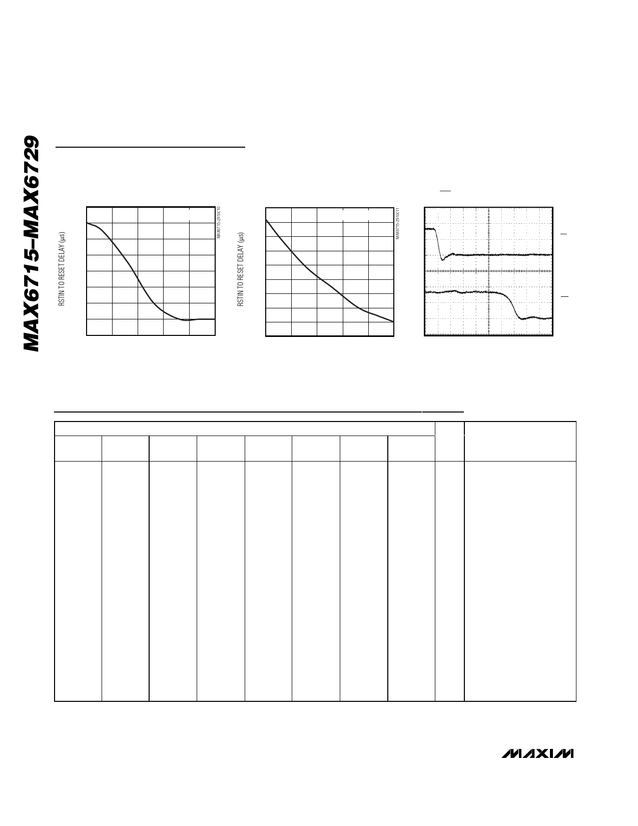
MR TO RESET OUTPUT DELAY
MAX6715-29 toc12
VMR
2V/div
50ns/div
VRST
2V/div
Pin Description
PIN
MAX6715/ MAX6717/
MAX6716 MAX6718
MAX6719/
MAX6720
MAX6721/
MAX6722
MAX6723/
MAX6724
MAX6725/
MAX6726
MAX6727
MAX6728/ NAME
MAX6729
FUNCTION
Active-Low Reset Output,
Open-Drain or Push-Pull.
RST/RST1 changes from
high to low when VCC1 or
VCC2 drops below the
selected reset thresholds,
RSTIN is below threshold,
MR is pulled low, or the
watchdog triggers a
1
1
1
1
1
1
1, 4
1
RST/
RST1
reset. RST/RST1 remains
low for the reset timeout
period after VCC1/
VCC2/RSTIN exceed the
device reset thresholds,
MR goes low to high, or
the watchdog triggers a
reset. Open-drain outputs
require an external pullup
resistor. Push-pull
outputs are referenced to
VCC1.
6 _______________________________________________________________________________________
Share Link: 