MAX6724 –ü—Ä–æ—Å–º–æ—Ç—Ä —Ç–µ—Ö–Ω–∏—á–µ—Å–∫–æ–≥–æ –æ–ø–∏—Å–∞–Ω–∏—è (PDF) - Maxim Integrated
–ù–æ–º–µ—Ä –≤ –∫–∞—Ç–∞–ª–æ–≥–µ
–ö–æ–º–ø–æ–Ω–µ–Ω—Ç—ã –û–ø–∏—Å–∞–Ω–∏–µ
–ø—Ä–æ–∏–∑–≤–æ–¥–∏—Ç–µ–ª—å
MAX6724 Datasheet PDF : 19 Pages
| |||
Dual/Triple Ultra-Low-Voltage SOT23 µP
Supervisory Circuits
A
VIN
R1
MAX6728/
MAX6729
PFI
PFO
R2
GND
B
VCC
R1
MAX6728/
MAX6729
PFI
PFO
R2
VIN
GND
( ) VTRIP = VPFI
R1 + R2
R2
[ ( ) ] VTRIP = R2
(VPFI)
1+
R1
1
R2
- VCC
R1
VPFI = 626.5mV
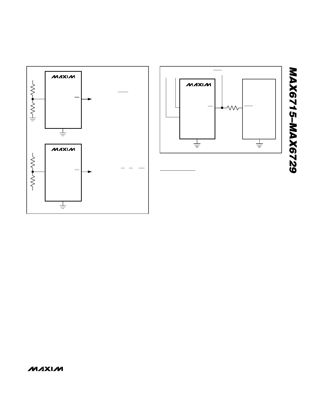
Figure 3. Using Power-Fail Input to Monitor an Additional
Power-Supply a) VIN is Positive b) VIN is Negative
providing an early power-fail warning so software can
conduct an orderly system shutdown. It can also be
used to monitor supplies other than VCC1 or VCC2 by
setting the power-fail threshold with a resistor-divider, as
shown in Figure 3. PFI is the input to the power-fail com-
parator. The typical comparator delay is 2µs from PFI to
PFO. Connect PFI to ground of VCC1 if unused.
Ensuring a Valid Reset Output
Down to VCC = 0
The MAX6715–MAX6729 are guaranteed to operate
properly down to VCC = 0.8V. In applications that
require valid reset levels down to VCC = 0 use a pull-
down resistor at RST to ground. The resistor value used
is not critical, but it must be large enough not to load
the reset output when VCC is above the reset threshold.
For most applications, 100kΩ is adequate. This config-
uration does not work for the open-drain outputs of the
MAX6715/MAX6717/MAX6719/MAX6721/MAX6723/
MAX6725/MAX6727/MAX6728. For push-pull, active-
high RST output connect the external resistor as a
pullup from RST to VCC1.
VCC1 VCC2
RESET TO OTHER SYSTEM COMPONENTS
MAX6715–
MAX6729
VCC2
RST
VCC1
4.7kΩ
µP
RESET
GND
GND
Figure 4. Interfacing to µPs with Bidirectional Reset I/O
Applications Information
Interfacing to µPs with Bidirectional
Reset Pins
Most microprocessors with bidirectional reset pins can
interface directly to open-drain RST output options.
Systems simultaneously requiring a push-pull RST out-
put and a bidirectional reset interface can be in logic
contention. To prevent contention, connect a 4.7kΩ
resistor between RST and the µP’s reset I/O port as
shown in Figure 4.
Adding Hysteresis to the Power-Fail
Comparator
The power-fail comparator has a typical input hysteresis
of 3mV. This is sufficient for most applications where a
power-supply line is being monitored through an external
voltage-divider (see the Power-Fail Comparator section).
If additional noise margin is desired, connect a resistor
between PFO and PFI as shown in Figure 5. Select the
values of R1, R2, and R3 so PFI sees VPFI (626mV) when
VEXT falls to its power-fail trip point (VFAIL) and when VIN
rises to its power-good trip point (VGOOD). The hysteresis
window extends between the specified VFAIL and VGOOD
thresholds. R3 adds the additional hysteresis by sinking
current from the R1/R2 divider network when PFO is logic
low and sourcing current into the network when PFO is
logic high. R3 is typically an order of magnitude greater
than R1 or R2.
The current through R2 should be at least 2.5µA to
ensure that the 25nA (max) PFI input current does not
significantly shift the trip points. Therefore, R2 <
VPFI/2.5µA < 248kΩ for most applications. R3 will provide
additional hysteresis for PFO push-pull (VOH = VCC1) or
open-drain (VOH = VPULLUP) applications.
______________________________________________________________________________________ 11
Share Link: 