3083 Просмотр технического описания (PDF) - Linear Technology
Номер в каталоге
Компоненты Описание
производитель
3083 Datasheet PDF : 28 Pages
| |||
LT3083
APPLICATIONS INFORMATION
Table 1 lists many common output voltages and the clos-
est standard 1% resistor values used to generate that
output voltage.
Regulation of the output voltage requires a minimum
load current of 1mA. For a true zero voltage output
operation, return this 1mA load current to a negative
supply voltage.
Table 1. 1% Resistors for Common Output Voltages
VOUT (V)
1
RSET (k)
20
1.2
24.3
1.5
30.1
1.8
35.7
2.5
49.9
3.3
66.5
5
100
With the lower level current used to generate the refer-
ence voltage, leakage paths to or from the SET pin can
create errors in the reference and output voltages. High
quality insulation should be used (e.g., Teflon, Kel-F);
cleaning of all insulating surfaces to remove fluxes and
other residues will probably be required. Surface coating
may be necessary to provide a moisture barrier in high
humidity environments.
Minimize board leakage by encircling the SET pin and
circuitry with a guard ring operated at a potential close
to itself. Tie the guard ring to the OUT pin. Guard rings
on both sides of the circuit board are required. Bulk leak-
age reduction depends on the guard ring width. 50nA
of leakage into or out of the SET pin and its associated
circuitry creates a 0.1% reference voltage error. Leakages
of this magnitude, coupled with other sources of leakage,
can cause significant offset voltage and reference drift,
especially over the possible operating temperature range.
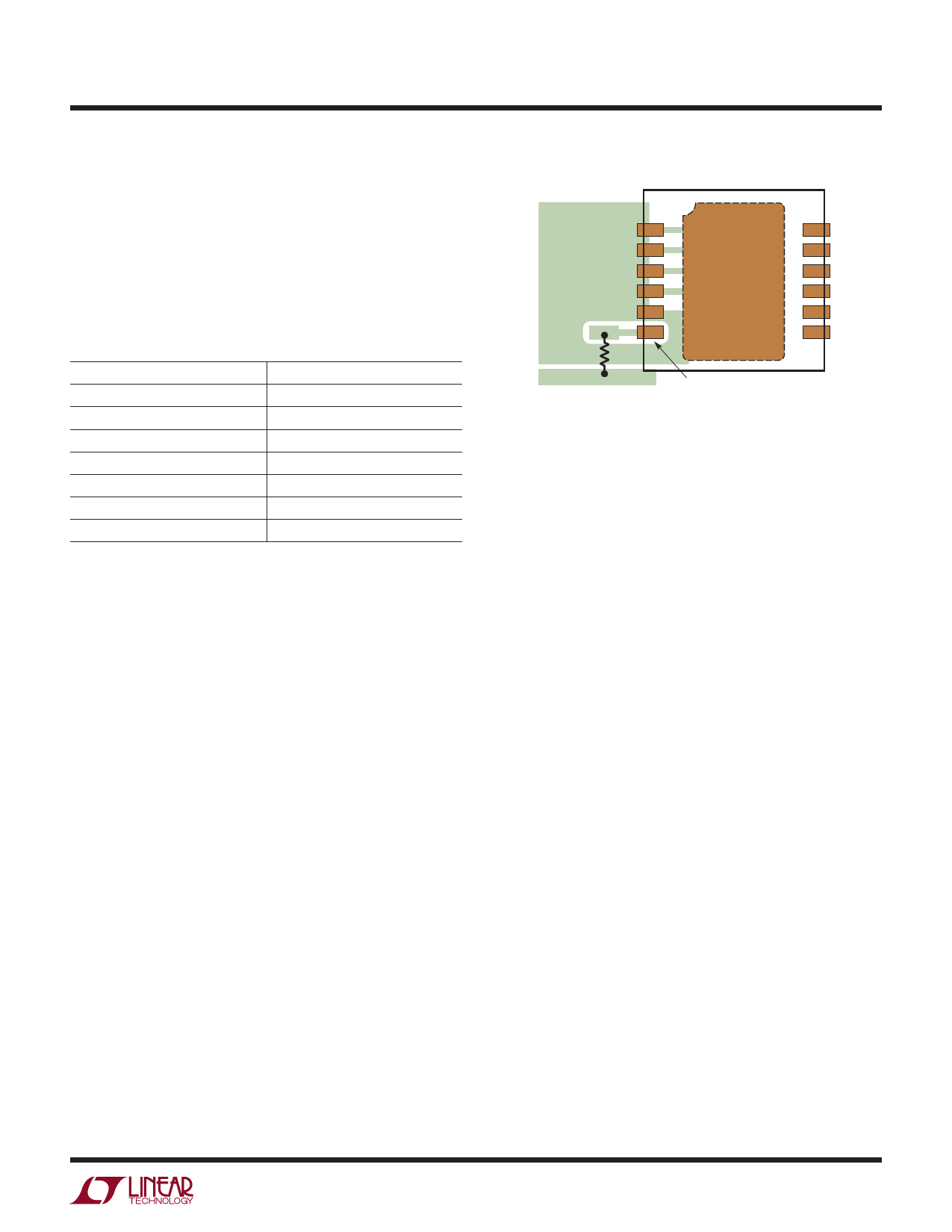
Figure 2 depicts an example of a guard ring layout.
If guard ring techniques are used, this bootstraps any
stray capacitance at the SET pin. Since the SET pin is
a high impedance node, unwanted signals may couple
into the SET pin and cause erratic behavior. This will
be most noticeable when operating with minimum
output capacitors at full load current. The easiest way
OUT
GND
SET PIN
3083 F02
Figure 2. Guard Ring Layout Example
for DF Package
to remedy this is to bypass the SET pin with a small
amount of capacitance from SET to ground, 10pF to
20pF is sufficient.
Stability and Input Capacitance
Typical minimum input capacitance is 10µF for IN and
2.2µF for VCONTROL. These amounts of capacitance work
well using low ESR ceramic capacitors when placed close
to the LT3083 and the circuit is located in close proximity
to the power source. Higher values of input capacitance
may be necessary to maintain stability depending on the
application.
Oscillating regulator circuits are often viewed as a problem
of phase margin and inadequate stability with the output
capacitor used. More and more frequently, the problem
is not the regulator operating without sufficient output
capacitance, but instead with too little input capacitance.
The entire circuit must be analyzed and debugged as a
whole; conditions relating to the input of the regulator
cannot be ignored.
The LT3083 input presents a high impedance to its power
source: the output voltage and load current are independent
of input voltage variations. To maintain stability of the
regulator circuit as a whole, the LT3083 must be powered
from a low impedance supply. When using short supply
lines or powering directly from a large switching supply,
there is no issue—hundreds or thousands of microfarads
of capacitance are available through a low impedance.
3083fa
11
Share Link: 