30TPS08-M3 Просмотр технического описания (PDF) - Vishay Semiconductors
Номер в каталоге
Компоненты Описание
производитель
30TPS08-M3 Datasheet PDF : 9 Pages
| |||
VS-30TPS..PbF Series, VS-30TPS..-M3 Series
www.vishay.com
Vishay Semiconductors
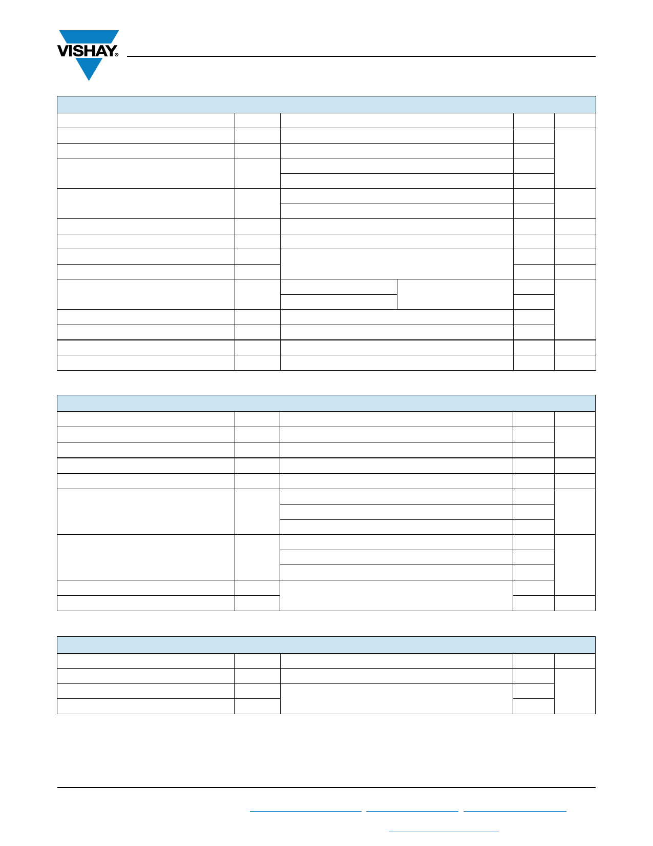
ABSOLUTE MAXIMUM RATINGS
PARAMETER
SYMBOL
Maximum average on-state current
Maximum RMS on-state current
IT(AV)
IRMS
Maximum peak, one-cycle
non-repetitive surge current
ITSM
Maximum I2t for fusing
I2t
Maximum I2t for fusing
Maximum on-state voltage drop
On-state slope resistance
Threshold voltage
I2t
VTM
rt
VT(TO)
Maximum reverse and direct leakage current IRM/IDM
Maximum holding current
Maximum latching current
Maximum rate of rise of off-state voltage
Maximum rate of rise of turned-on current
IH
IL
dV/dt
dI/dt
TEST CONDITIONS
VALUES
TC = 95 °C, 180° conduction half sine wave
20
30
10 ms sine pulse, rated VRRM applied
250
10 ms sine pulse, no voltage reapplied
300
10 ms sine pulse, rated VRRM applied
310
10 ms sine pulse, no voltage reapplied
442
t = 0.1 to 10 ms, no voltage reapplied
4420
20 A, TJ = 25 °C
1.3
12
TJ = 125 °C
1.0
TJ = 25 °C
TJ = 125 °C
0.5
VR = Rated VRRM/VDRM
10
Anode supply = 6 V, resistive load, initial IT = 1 A, TJ = 25 °C 150
Anode supply = 6 V, resistive load, TJ = 25 °C
200
TJ = TJ maximum, linear to 80 % VDRM, Rg-k = Open
500
150
UNITS
A
A2s
A2s
V
m
V
mA
V/µs
A/µs
TRIGGERING
PARAMETER
Maximum peak gate power
Maximum average gate power
Maximum peak positive gate current
Maximum peak negative gate voltage
SYMBOL
PGM
PG(AV)
+ IGM
- VGM
Maximum required DC gate current to trigger IGT
Maximum required DC gate
voltage to trigger
VGT
Maximum DC gate voltage not to trigger
VGD
Maximum DC gate current not to trigger
IGD
TEST CONDITIONS
Anode supply = 6 V, resistive load, TJ = - 10 °C
Anode supply = 6 V, resistive load, TJ = 25 °C
Anode supply = 6 V, resistive load, TJ = 125 °C
Anode supply = 6 V, resistive load, TJ = - 10 °C
Anode supply = 6 V, resistive load, TJ = 25 °C
Anode supply = 6 V, resistive load, TJ = 125 °C
TJ = 125 °C, VDRM = Rated value
VALUES
8.0
2.0
1.5
10
60
45
20
2.5
2.0
1.0
0.25
2.0
UNITS
W
A
V
mA
V
mA
SWITCHING
PARAMETER
Typical turn-on time
Typical reverse recovery time
Typical turn-off time
SYMBOL
tgt
trr
tq
TJ = 25 °C
TJ = 125 °C
TEST CONDITIONS
VALUES
0.9
4
110
UNITS
µs
Revision: 29-Jul-13
2
Document Number: 94386
For technical questions within your region: DiodesAmericas@vishay.com, DiodesAsia@vishay.com, DiodesEurope@vishay.com
THIS DOCUMENT IS SUBJECT TO CHANGE WITHOUT NOTICE. THE PRODUCTS DESCRIBED HEREIN AND THIS DOCUMENT
ARE SUBJECT TO SPECIFIC DISCLAIMERS, SET FORTH AT www.vishay.com/doc?91000
Share Link: 