SST27SF010-90-3C-NG Просмотр технического описания (PDF) - Silicon Storage Technology
Номер в каталоге
Компоненты Описание
производитель
SST27SF010-90-3C-NG
Silicon Storage Technology

SST27SF010-90-3C-NG Datasheet PDF : 23 Pages
| |||
512 Kbit / 1 Mbit / 2 Mbit Many-Time Programmable Flash
SST27SF512 / SST27SF010 / SST27SF020
Data Sheet
Absolute Maximum Stress Ratings (Applied conditions greater than those listed under “Absolute Maximum
Stress Ratings” may cause permanent damage to the device. This is a stress rating only and functional operation
of the device at these conditions or conditions greater than those defined in the operational sections of this data
sheet is not implied. Exposure to absolute maximum stress rating conditions may affect device reliability.)
Temperature Under Bias . . . . . . . . . . . . . . . . . . . . . . . . . . . . . . . . . . . . . . . . . . . . . . . . . . . . . . . . . -55°C to +125°C
Storage Temperature . . . . . . . . . . . . . . . . . . . . . . . . . . . . . . . . . . . . . . . . . . . . . . . . . . . . . . . . . . . -65°C to +150°C
D. C. Voltage on Any Pin to Ground Potential . . . . . . . . . . . . . . . . . . . . . . . . . . . . . . . . . . . . . . . . -0.5V to VDD+0.5V
Transient Voltage (<20 ns) on Any Pin to Ground Potential . . . . . . . . . . . . . . . . . . . . . . . . . . . . . -2.0V to VDD+2.0V
Voltage on A9 and VPP Pin to Ground Potential . . . . . . . . . . . . . . . . . . . . . . . . . . . . . . . . . . . . . . . . . -0.5V to 14.0V
Package Power Dissipation Capability (TA = 25°C) . . . . . . . . . . . . . . . . . . . . . . . . . . . . . . . . . . . . . . . . . . . . . . 1.0W
Through Hole Lead Soldering Temperature (10 Seconds) . . . . . . . . . . . . . . . . . . . . . . . . . . . . . . . . . . . . . . . 300°C
Surface Mount Solder Reflow Temperature1 . . . . . . . . . . . . . . . . . . . . . . . . . . . . . . . . . . . . . . 260°C for 10 seconds
Output Short Circuit Current2 . . . . . . . . . . . . . . . . . . . . . . . . . . . . . . . . . . . . . . . . . . . . . . . . . . . . . . . . . . . . 100 mA
1. Excluding certain with-Pb 32-PLCC units, all packages are 260°C capable in both non-Pb and with-Pb solder versions.
Certain with-Pb 32-PLCC package types are capable of 240°C for 10 seconds; please consult the factory for the latest information.
2. Outputs shorted for no more than one second. No more than one output shorted at a time.
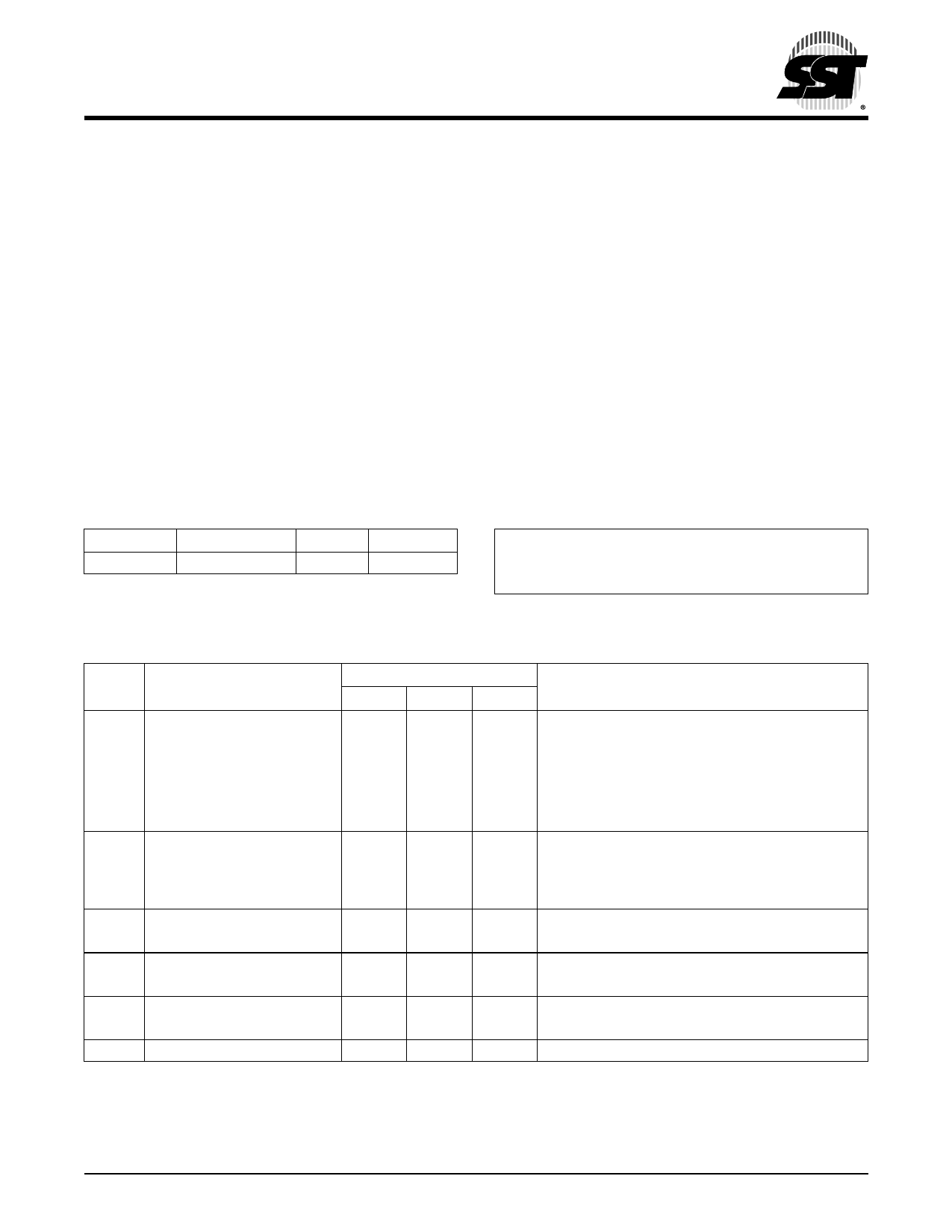
OPERATING RANGE
Range
Ambient Temp
Commercial 0°C to +70°C
VDD
4.5-5.5V
VPP
11.4-12V
AC CONDITIONS OF TEST
Input Rise/Fall Time . . . . . . . . . . . 10 ns
Output Load . . . . . . . . . . . . . . . . . CL = 30 pF for 70 ns
See Figures 9 and 10
TABLE 5: READ MODE DC OPERATING CHARACTERISTICS FOR SST27SF512/010/020
VDD = 4.5-5.5V, VPP=VDD OR VSS (TA = 0°C TO +70°C (COMMERCIAL))
Limits
Symbol Parameter
Min
Max Units Test Conditions
IDD
VDD Read Current
IPPR
VPP Read Current
ISB1
Standby VDD Current
(TTL input)
Address input=VILT/VIHT at f=1/TRC Min
VDD=VDD Max
30
mA CE#=OE#=VIL, all I/Os open
Address input=VILT/VIHT at f=1/TRC Min
VDD=VDD Max, VPP=VDD
100
µA CE#=OE#=VIL, all I/Os open
3
mA CE#=VIH, VDD=VDD Max
ISB2
Standby VDD Current
(CMOS input)
ILI
Input Leakage Current
ILO
Output Leakage Current
VIL
Input Low Voltage
VIH
Input High Voltage
VOL
Output Low Voltage
VOH
Output High Voltage
IH
Supervoltage Current for A9
100
µA CE#=VDD-0.3
VDD=VDD Max
1
µA VIN=GND to VDD, VDD=VDD Max
10
µA VOUT=GND to VDD, VDD=VDD Max
0.8
V
VDD=VDD Min
2.0 VDD+0.5
V
VDD=VDD Max
0.2
V
IOL=2.1 mA, VDD=VDD Min
2.4
V
IOH=-400 µA, VDD=VDD Min
200
µA CE#=OE#=VIL, A9=VH Max
T5.6 1152
©2005 Silicon Storage Technology, Inc.
7
S71152-11-000
9/05
Share Link: