AD6643 Просмотр технического описания (PDF) - Analog Devices
Номер в каталоге
Компоненты Описание
производитель
AD6643 Datasheet PDF : 40 Pages
| |||
AD6643
Data Sheet
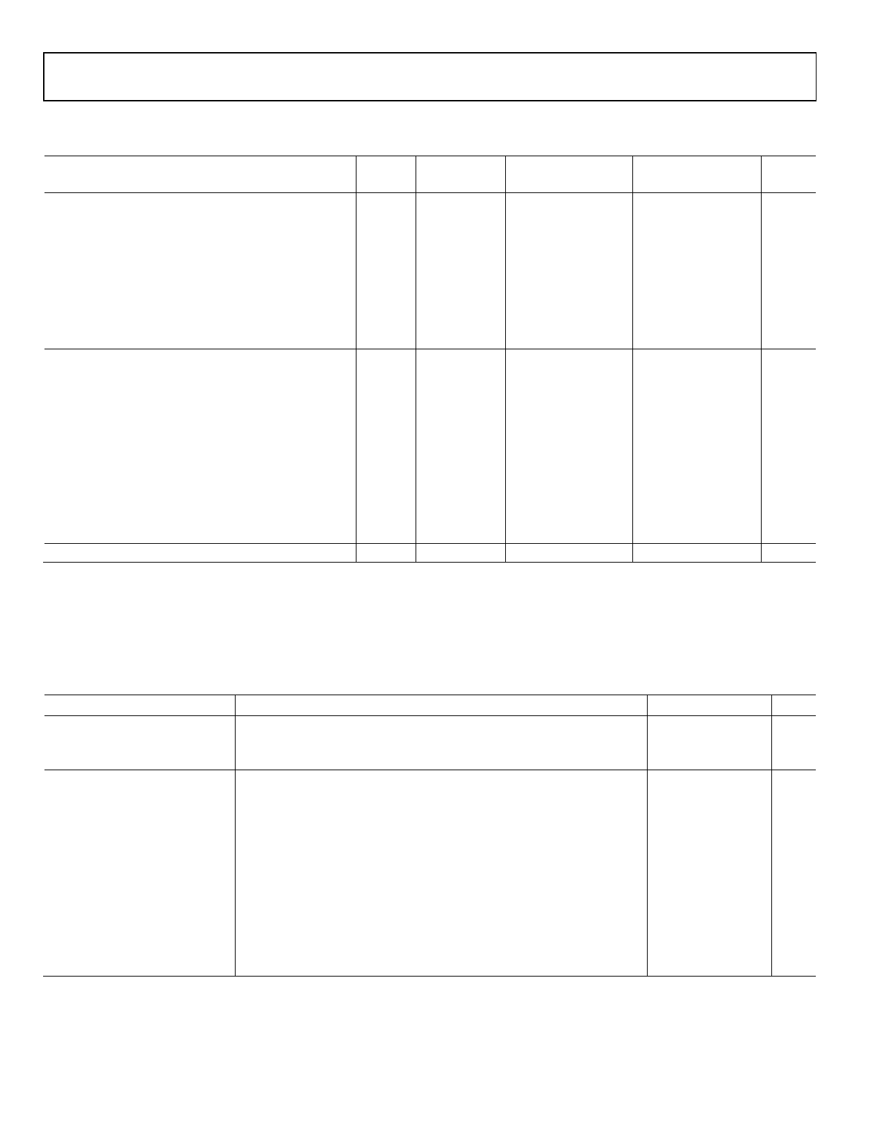
SWITCHING SPECIFICATIONS
Table 4.
Parameter
CLOCK INPUT PARAMETERS
Input Clock Rate
Conversion Rate1
CLK Period—Divide-by-1 Mode2
CLK Pulse Width High2
Divide-by-1 Mode, DCS Enabled
Divide-by-1 Mode, DCS Disabled
Divide-by-2 Through Divide-by-8 Modes, DCS
Enabled
DATA OUTPUT PARAMETERS (DATA, OR)
LVDS Mode
Data Propagation Delay2
DCO Propagation Delay2
DCO to Data Skew2
Pipeline Delay (Latency)
NSR Enabled
Aperture Delay4
Aperture Uncertainty (Jitter)4
Wake-Up Time (from Standby)
Wake-Up Time (from Power-Down)
OUT-OF-RANGE RECOVERY TIME
1 Conversion rate is the clock rate after the divider.
2 See Figure 2 for timing diagram.
3 Cycles refers to ADC input sample rate cycles.
4 Not shown in timing diagrams.
AD6643-200
AD6643-250
Symbol Temperature Min Typ Max Min Typ Max Unit
Full
Full
tCLK
Full
tCH
Full
Full
Full
tPD
Full
tDCO
Full
tSKEW
Full
Full
Full
tA
Full
tJ
Full
Full
Full
Full
625
40
200 40
4.0
4
625 MHz
250 MSPS
ns
2.25 2.5 2.75 1.8 2.0 2.2 ns
2.375 2.5 2.625 1.9 2.0 2.1 ns
0.8
0.8
ns
1.0
0.1
6.0
6.0
ns
6.7
6.7
ns
0.4 0.7 1.0 0.4 0.7 1.0 ns
10
10
Cycles3
13
13
Cycles3
1.0
1.0
ns
0.1
0.1
ps rms
10
10
μs
250
250
μs
3
3
Cycles
TIMING SPECIFICATIONS—AD6643-200/AD6643-250
Table 5.
Parameter
SYNC TIMING REQUIREMENTS
tSSYNC
tHSYNC
SPI TIMING REQUIREMENTS
tDS
tDH
tCLK
tS
tH
tHIGH
tLOW
tEN_SDIO
tDIS_SDIO
Conditions
See Figure 3 for timing details
SYNC to the rising edge of CLK setup time
SYNC to the rising edge of CLK hold time
See Figure 59 for SPI timing diagram
Setup time between the data and the rising edge of SCLK
Hold time between the data and the rising edge of SCLK
Period of the SCLK
Setup time between CSB and SCLK
Hold time between CSB and SCLK
Minimum period that SCLK should be in a logic high state
Minimum period that SCLK should be in a logic low state
Time required for the SDIO pin to switch from an input to an output
relative to the SCLK falling edge (not shown in Figure 59)
Time required for the SDIO pin to switch from an output to an input
relative to the SCLK rising edge (not shown in Figure 59)
Min Typ Max Unit
0.3
ns
0.4
ns
2
ns
2
ns
40
ns
2
ns
2
ns
10
ns
10
ns
10
ns
10
ns
Rev. C | Page 8 of 40
Share Link: 