MAX19700 Просмотр технического описания (PDF) - Maxim Integrated
Номер в каталоге
Компоненты Описание
производитель
MAX19700 Datasheet PDF : 32 Pages
| |||
7.5Msps, Ultra-Low-Power
Analog Front-End
ELECTRICAL CHARACTERISTICS (continued)
(VDD = 3V, OVDD = 1.8V, internal reference (1.024V), CL ≈ 10pF on all digital outputs, fCLK = 7.5MHz (50% duty cycle), ADC input
amplitude = -0.5dBFS, DAC output amplitude = 0dBFS, differential ADC input, differential DAC output, CREFP = CREFN = CCOM =
0.33µF. Typical values are at TA = +25°C, unless otherwise noted. CL < 5pF on all aux-DAC outputs.) (Note 1)
PARAMETER
DIGITAL OUTPUTS (D0–D9, DR)
SYMBOL
CONDITIONS
MIN TYP MAX UNITS
Output-Voltage Low
VOL
ISINK = 200µA
0.2 x
OVDD
V
Output-Voltage High
VOH
ISOURCE = 200µA
0.8 x
OVDD
V
Tri-State Leakage Current
Tri-State Output Capacitance
ILEAK
COUT
-1
+1
µA
5
pF
Note 1: Specifications from TA = +25°C to +85°C are guaranteed by production tests. Specifications from TA = +25°C to -40°C are
guaranteed by design and characterization.
Note 2: The minimum clock frequency for the MAX19700 is 2MHz.
Note 3: SNR, SINAD, SFDR, HD3, and THD are based on a differential analog input voltage of -0.5dBFS referenced to the amplitude
of the digital outputs. SINAD and THD are calculated using HD2 through HD6.
Note 4: Crosstalk rejection is measured by applying a high-frequency test tone to one channel and a low-frequency tone to the second
channel. FFTs are performed on each channel. The parameter is specified as the power ratio of the first and second channel
FFT test tone.
Note 5: Amplitude and phase matching is measured by applying the same signal to each channel, and comparing the two output
signals using a sine-wave fit.
Note 6: Guaranteed by design and characterization.
Typical Operating Characteristics
(VDD = 3V, OVDD = 1.8V, internal reference (1.024V), CL ≈ 10pF on all digital outputs, fCLK = 7.5MHz 50% duty cycle, ADC input
amplitude = -0.5dBFS, DAC output amplitude = 0dBFS, differential ADC input, differential DAC output, CREFP = CREFN = CCOM =
0.33µF, TA = +25°C, unless otherwise noted.)
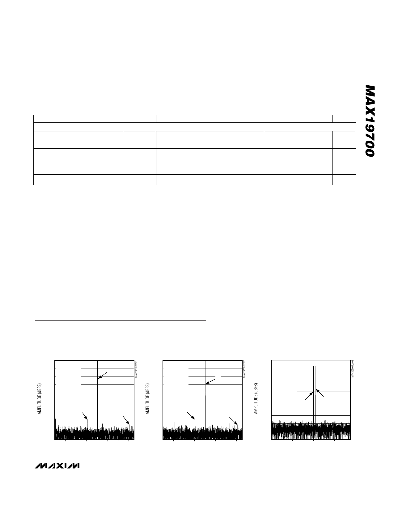
Rx ADC CHANNEL-IA FFT PLOT
0
fCLK = 7.5MHz
-10 fIA = 2MHz
-20
AIA = -0.5dBFS
8192-POINT
IA
-30 DATA RECORD
-40
-50
Rx ADC CHANNEL-QA FFT PLOT
0
fCLK = 7.5MHz
-10 fQA = 2MHz
-20
AQA = -0.5dBFS
8192-POINT
QA
-30 DATA RECORD
-40
-50
Rx ADC CHANNEL-IA
TWO-TONE FFT PLOT
0
fCLK = 7.5MHz
-10 f1 = 2.0MHz
-20
f2 = 2.1MHz
AIA = -7dBFS
-30 PER TONE
8192-POINT
-40 DATA RECORD
-50
f1
f2
-60
HD3
-70
-60
HD2
HD3
-70
-60
HD2
-70
-80
-80
-80
-90
-90
-90
-100
0
0.5 1.0 1.5 2.0 2.5 3.0 3.5
FREQUENCY (MHz)
-100
0
0.5 1.0 1.5 2.0 2.5 3.0 3.5
FREQUENCY (MHz)
-100
0
0.5 1.0 1.5 2.0 2.5 3.0 3.5
FREQUENCY (MHz)
_______________________________________________________________________________________ 9
Share Link: 