S3C7324 Просмотр технического описания (PDF) - Samsung
Номер в каталоге
Компоненты Описание
производитель
S3C7324 Datasheet PDF : 37 Pages
| |||
S3C7324/P7324
PRODUCT OVERVIEW
PIN DESCRIPTIONS
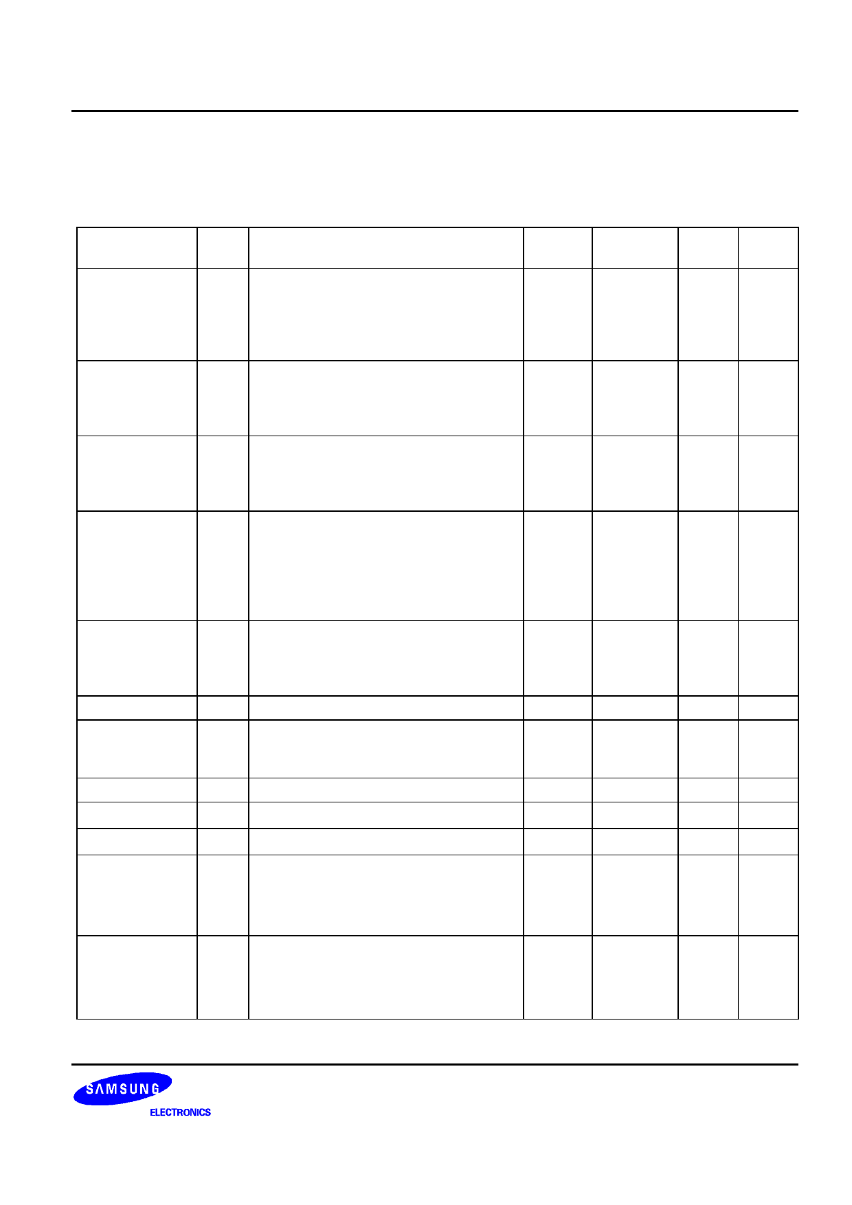
Pin Name
P1.0
P1.1
P1.2
P1.3
P2.0
P2.1
P2.2
P2.3
P3.0
P3.1
P3.2
P3.3
P4.0–P4.3
P5.0–P5.3
P6.0
P6.1
P6.2
P6.3
SEG0–SEG19
P8.0–P8.3
P9.0–P9.3
COM0–COM3
VDD
VSS
XOUT, XIN
XTOUT, XTIN
Table 1-1. S3C7324 Pin Descriptions
Pin
Type
Description
Number
I/O 4-bit I/O port.
17
1-bit or 4-bit read, write, and test are
18
possible. Each pin can be specified as
19
input or output port. Pull-up resistors can 20
be configured by software.
I 4-bit input port. 1-bit and 4-bit read and
1
test are possible.
2
Pull-up resistors can be configured by
3
software.
4
I 4-bit input port.
5
1-bit and 4-bit read and test are possible
6
Pull-up resistors can be configured by
7
software.
8
I/O 4-bit I/O ports. N-channel open-drain
output up to 5 V. 1-bit and 4-bit read,
write, and test are possible. Ports 4 and
5 can be paired to support 8-bit data.
Pull-up resistors can be configured by
software.
21–24
25–28
I/O 1-bit and 4-bit read, write, and test are
29
possible. Each pin can be specified as
30
input or output port. Pull-up resistors can
31
be configured by software.
32
O LCD segment signal output
60–41
O 4-bit output ports. 1-bit and 4-bit write
and test are possible. Ports 8 and 9 can
be paired to support 8-bit data.
33–36
37–40
O LCD common signal output
64–61
– Main power supply
9
– Main ground
10
– Crystal, ceramic, or RC oscillator pins for 11,12
main system clock. (For external clock
input, use XIN and input XIN's reverse
phase to XOUT)
– Crystal oscillator pin for a subsystem
15,14
clock. (For external clock input, use XTIN
and input XTIN's reverse phase to
XTOUT)
Share
Pin
INT0
INT1
INT2
INT4
Reset
Value
Input
Circuit
Type
D-4
–
–
FMF
AMF
ADC0
ADC1
ADC2
ADC3
–
–
Input
Input
A-4
A-4
B-4
B-4
F-13
Input E-2
BUZ
KS0
KS1
KS2
–
SEG27–
SEG20
Input
Output
Output
D-2
D-4
D-4
D-4
H-16
H-16
–
Output H-16
–
–
–
–
–
–
–
–
–
–
–
–
1-5
Share Link: 