S1M8662A Просмотр технического описания (PDF) - Samsung
Номер в каталоге
Компоненты Описание
производитель
S1M8662A Datasheet PDF : 22 Pages
| |||
S1M8662A (Preliminary)
RX IF/BBA WITH GPS
AC Characteristics (Continued)
Characteristic
Single-tone
jammer desense
Residual
Sideband
Test Conditions
Overall gain reduction due to one jammer.
The in-band signal at -97dBm (control the
AGC control voltage to 0.5*F/S)and the
jammer signal at 900kHz and -57dBm are
simultaneously input.
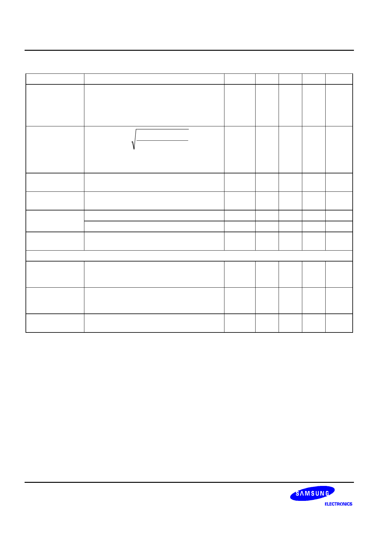
RSB = 20log
1 + k 2 + 2k cosθ
1 + k 2 − 2k cosθ
Symbol Min Typ Max Unit
Jdsen
-
-
1.0
dB
RSB
22
dB
k : Linear Gain Mismatch
θ : Phase Mismatch in Deg.
Offset gain slope Amount of code change of the voltage ADC
GOFS
-
250
- %FS/V
output at the I/Q offset control
Offset adjust
-
input impedance
Zoff 100 -
-
kΩ
Out-band
≥ 900kHz
ATC9 46
-
-
dB
attenuation
≥ 1.2MHz
ATC12 48
-
-
dB
Gain flatness
Amount of gain change along I and Q paths
Gft
-1
between 1kHz to 615kHz
1
dB
IF VCO pertormance
VCO and
buffered output
Frequency range
VCO external time constant and PLL value
Fvco
-
170 500 MHz
VCO phase noise Tank LC's Q value should be above 20.
Measure @100kHz away from the mid-
frequency.
Pvco
-
-
104 dBc/Hz
RXVCO_OUT
Select a VCO buffer output value reduced by Ovco -15
-
output power
-2dB. Connect output load to 50Ω.
-
dBm
8
Share Link: 