CY7C1318V18 Просмотр технического описания (PDF) - Cypress Semiconductor
Номер в каталоге
Компоненты Описание
производитель
CY7C1318V18 Datasheet PDF : 24 Pages
| |||

PRELIMINARY
CY7C1316V18
CY7C1318V18
CY7C1320V18
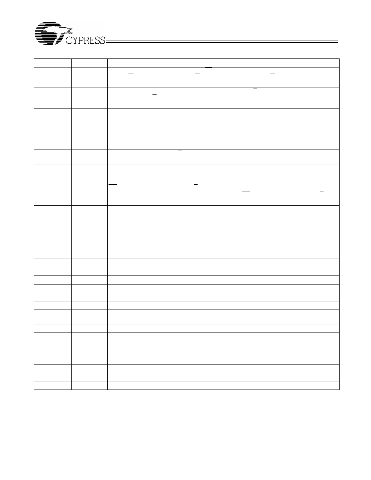
Pin Definitions (continued)
Pin Name
R/W
C
C
K
K
CQ
CQ
ZQ
DOFF
TDO
TCK
TDI
TMS
NC
NC/36M
NC/72M
VSS/72M
VSS/144M
VSS/288M
VREF
VDD
VSS
VDDQ
I/O
Pin Description
Input- Synchronous Read/Write Input. When LD is LOW, this input designates the access type (READ
Synchronous when R/W is HIGH, WRITE when R/W is low) for loaded address. R/W must meet the set-up and
hold times around edge of K.
Input-
Clock
Positive Output Clock Input. C is used in conjunction with C to clock out the Read data from
the device. C and C can be used together to deskew the flight times of various devices on the
board back to the controller. See application example for further details.
Input-
Clock
Negative Output Clock Input. C is used in conjunction with C to clock out the Read data from
the device. C and C can be used together to deskew the flight times of various devices on the
board back to the controller. See application example for further details.
Input-
Clock
Positive Input Clock Input. The rising edge of K is used to capture synchronous inputs to the
device and to drive out data through Q[x:0] when in single clock mode. All accesses are initiated
on the rising edge of K.
Input-
Clock
Echo Clock
Negative Input Clock Input. K is used to capture synchronous data being presented to the device
and to drive out data through Q[x:0] when in single clock mode.
CQ is referenced with respect to C. This is a free running clock and is synchronized to the
output clock of the QDRTM-II. In the single clock mode, CQ is generated with respect to K. The
timings for the echo clocks are shown in the AC timing table.
Echo Clock CQ is referenced with respect to C. This is a free running clock and is synchronized to the
output clock of the QDRTM-II. In the single clock mode, CQ is generated with respect to K. The
timings for the echo clocks are shown in the AC timing table.
Input
Output Impedance Matching Input. This input is used to tune the device outputs to the system
data bus impedance. Q[x:0] output impedance are set to 0.2 x RQ, where RQ is a resistor
connected between ZQ and ground. Alternately, this pin can be connected directly to VDD, which
enables the minimum impedance mode. This pin cannot be connected directly to GND or left
unconnected.
Input
DLL Turn Off. Connecting this pin to ground will turn off the DLL inside the device. The timings
in the DLL turned off operation will be different from those listed in this data sheet. More details
on this operation can be found in the application note, “DLL Operation in the QDRTM-II.”
Output TDO for JTAG.
Input TCK pin for JTAG.
Input TDI pin for JTAG.
Input TMS pin for JTAG.
Input No connects. Can be tied to any voltage level.
Input Address expansion for 36M. This is not connected to the die.
Input
Address expansion for 72M. This is not connected to the die and so can be tied to any voltage
level.
Input Address expansion for 72M. This must be tied LOW on the 18M SRAM.
Input Address expansion for 144M. This must be tied LOW on the 18M SRAM.
Input Address expansion for 288M. This must be tied LOW on the 18M SRAM.
Input- Reference Voltage Input. Static input used to set the reference level for HSTL inputs and Outputs
Reference as well as A/C measurement points.
Power Supply Power supply inputs to the core of the device. Should be connected to 1.8V power supply.
Ground Ground for the device. Should be connected to ground of the system.
Power Supply Power supply inputs for the outputs of the device. Should be connected to 1.5V power supply.
Document #: 38-05177 Rev. *A
Page 5 of 24