PBL40215 Просмотр технического описания (PDF) - Ericsson
Номер в каталоге
Компоненты Описание
производитель
PBL40215 Datasheet PDF : 22 Pages
| |||
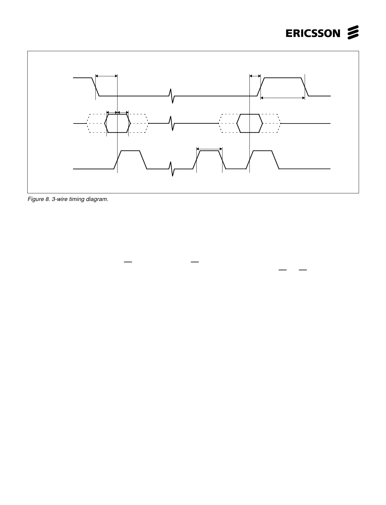
PBL 402 15
tSCK
ST
tDS tDH
D
MSB
CK
Clock enabled
tCKW
tDS
tSW
Clock disabled
LSB
Figure 8. 3-wire timing diagram.
Word A.
Description.
Word A has the address W0 = 0. It permits IC operation and defines the synthesiser frequency.
IC operation is controlled by the EN pin and the CE flag. If EN is not active then CE must be enabled for the IC to become
and remain operational. If CE is disabled then the IC shuts down completely with only the status of ST and EN determining if the
control section takes power. All configurations are erased and must be re-programmed if the chip has been disabled.
CL determines if the internal flags or the hard wire control lines are used to control section power. The internal flags provide
more flexibility.
10
Share Link: 