LPS3015 Просмотр технического описания (PDF) - Microchip Technology
Номер в каталоге
Компоненты Описание
производитель
LPS3015 Datasheet PDF : 38 Pages
| |||
MCP16301
1.0 ELECTRICAL
CHARACTERISTICS
Absolute Maximum Ratings †
VIN, SW ............................................................... -0.5V to 40V
BOOST – GND ................................................... -0.5V to 46V
BOOST – SW Voltage........................................ -0.5V to 6.0V
VFB Voltage ........................................................ -0.5V to 6.0V
EN Voltage ............................................. -0.5V to (VIN + 0.3V)
Output Short Circuit Current ................................. Continuous
Power Dissipation ....................................... Internally Limited
Storage Temperature ................................... -65°C to +150°C
Ambient Temperature with Power Applied ..... -40°C to +85°C
Operating Junction Temperature.................. -40°C to +125°C
ESD Protection On All Pins:
HBM ................................................................. 3 kV
MM .................................................................200 V
† Notice: Stresses above those listed under “Maximum
Ratings” may cause permanent damage to the device.
This is a stress rating only and functional operation of
the device at those or any other conditions above those
indicated in the operational sections of this
specification is not intended. Exposure to maximum
rating conditions for extended periods may affect
device reliability.
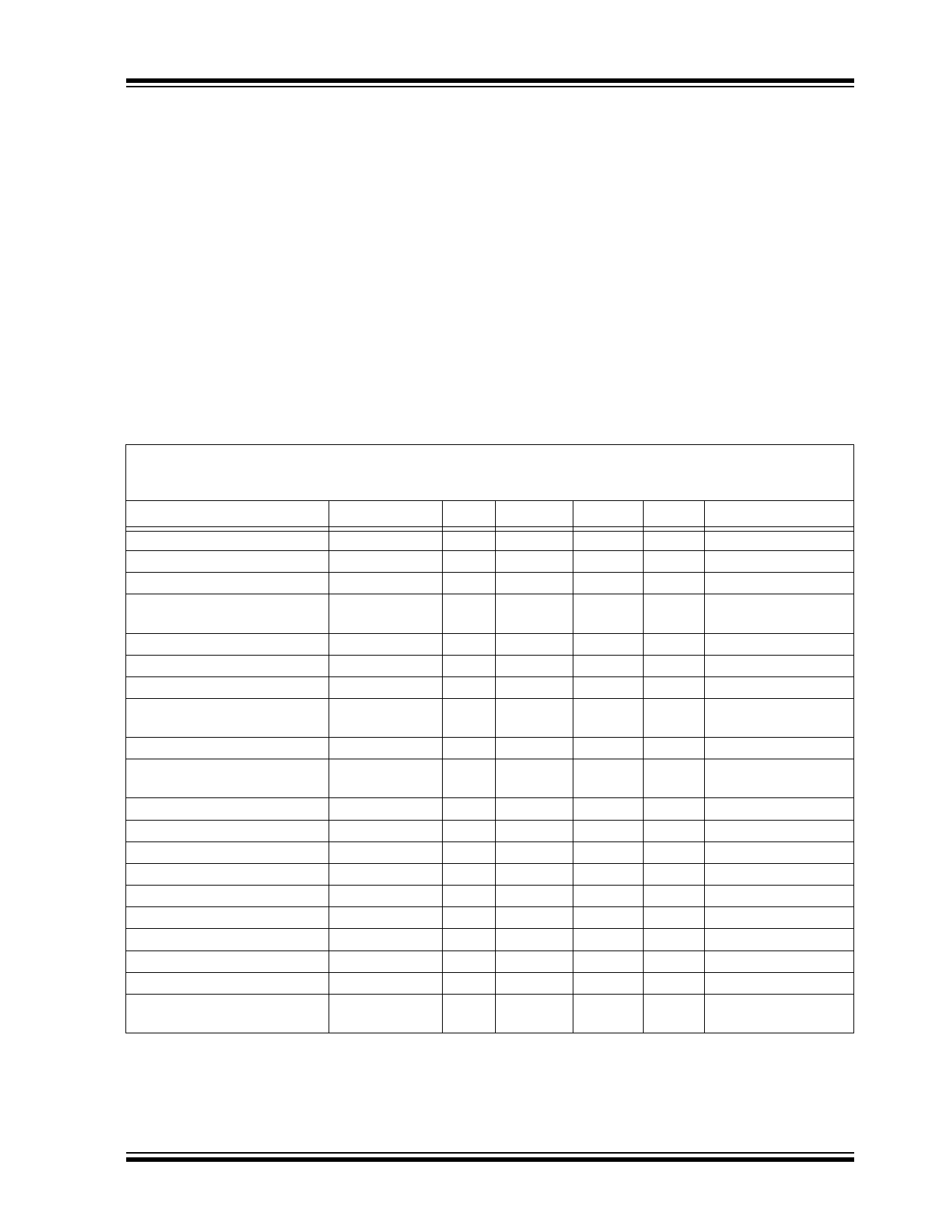
DC CHARACTERISTICS
Electrical Characteristics: Unless otherwise indicated, TA = +25°C, VIN = VEN = 12V, VBOOST - VSW = 3.3V,
VOUT = 3.3V, IOUT = 100 mA, L = 15 µH, COUT = CIN = 2 X 10 µF X7R Ceramic Capacitors
Boldface specifications apply over the TA range of -40oC to +85oC.
Parameters
Sym
Min
Typ
Max Units
Conditions
Input Voltage
Feedback Voltage
Output Voltage Adjust Range
Feedback Voltage
Line Regulation
VIN
VFB
VOUT
(ΔVFB/VFB)/ΔVIN
—
0.784
2.0
—
4.0
0.800
—
0.01
30
0.816
15.0
0.1
V Note 1
V
V Note 2
%/V VIN = 12V to 30V;
Feedback Input Bias Current
Undervoltage Lockout Start
Undervoltage Lockout Stop
Undervoltage Lockout
Hysteresis
IFB
-250
±10
UVLOSTRT
—
3.5
UVLOSTOP
2.4
3.0
UVLOHYS
—
0.4
+250
4.0
—
—
nA
V VIN Rising
V VIN Falling
V
Switching Frequency
fSW
425
500
550
kHz IOUT = 200 mA
Maximum Duty Cycle
DCMAX
90
95
—
% VIN = 5V; VFB = 0.7V;
IOUT = 100 mA
Minimum Duty Cycle
DCMIN
—
1
—
%
NMOS Switch On Resistance
RDS(ON)
—
0.46
—
Ω VBOOST - VSW = 3.3V
NMOS Switch Current Limit
IN(MAX)
—
1.3
—
A VBOOST - VSW = 3.3V
Quiescent Current
IQ
—
2
7.5
mA VBOOST= 3.3V; Note 3
Quiescent Current - Shutdown
IQ
—
7
10
µA VOUT = EN = 0V
Maximum Output Current
IOUT
600
—
—
mA Note 1
EN Input Logic High
VIH
1.4
—
—
V
EN Input Logic Low
VIL
—
—
0.4
V
EN Input Leakage Current
IENLK
—
0.05
1.0
µA VEN = 12V
Soft-Start Time
tSS
—
150
—
µS EN Low to High,
90% of VOUT
Note 1: The input voltage should be > output voltage + headroom voltage; higher load currents increase the input voltage
necessary for regulation. See characterization graphs for typical input to output operating voltage range.
2: For VIN < VOUT, VOUT will not remain in regulation.
3: VBOOST supply is derived from VOUT.
© 2011 Microchip Technology Inc.
DS25004A-page 3
Share Link: 