MN6732741 Просмотр технического описания (PDF) - Panasonic Corporation
Номер в каталоге
Компоненты Описание
производитель
MN6732741
Panasonic Corporation

MN6732741 Datasheet PDF : 15 Pages
| |||
MN6732741
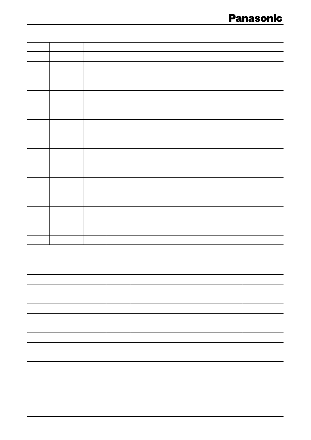
I Pin Descriptions (continued)
Pin No.
Pin
I/O
Description
109
DIN4
I Digital signal input
110
VDD4
VDD Digital system power supply (3.3 V)
111
VSS4
VSS Digital system ground
112
DIN3
I Digital signal input
113
DIN2
I Digital signal input
114
DIN1
I Digital signal input
115
DIN0
I Digital signal input (LSB)
116
DS2
O CDS pulse 1
117
DS1
O CDS pulse 2
118 TESTDC2
I Test input (Normally connect to low.)
119 TESTSW5
I Test input (Normally connect to low.)
120
R
O φR pulse
121
N.C.
122
TGVDD VDD TG power supply
123
TGVSS
VSS TG ground
124
N.C.
125
H2
O φH1 transfer pulse
126
N.C.
127
H1
O φH2 transfer pulse
128
N.C.
I Electrical Characteristics
1. Absolute Maximum Ratings
Parameter
Symbol
Rating
Unit
Supply voltage (digital)
VDD
− 0.3 to +4.6
V
Supply voltage (analog)
AVDD
− 0.3 to +4.6
V
Input voltage
VI
− 0.3 to VDD+0.3
V
Output voltage
VO
− 0.3 to VDD+0.3
V
Output current
IO
±48
mA
Power dissipation
PD
750
mW
Operating temperature
Topr
−20 to +70
°C
Storage temperature
Tstg
−55 to +150
°C
Note) 1. The absolute maximum ratings are limit values for stresses applied to the chip so that the chip will not be destroyed.
Operation is not guaranteed within these ranges.
2. Always apply the identical potential to the following pins: VDD1, VDD2, VDD3, VDD4, VDD5, VDDTG, ADVDD, DAVDD1,
and DAVDD2.
Always apply the identical potential to the following pins: VSS1, VSS2, VSS3, VSS4, VSS5, VSSTG, ADVSS, DAVSS1,
and DAVSS2.
8
SDB00060AEM
Share Link: