MAX691AD Просмотр технического описания (PDF) - Maxim Integrated
Номер в каталоге
Компоненты Описание
производитель
MAX691AD Datasheet PDF : 16 Pages
| |||

Microprocessor Supervisory Circuits
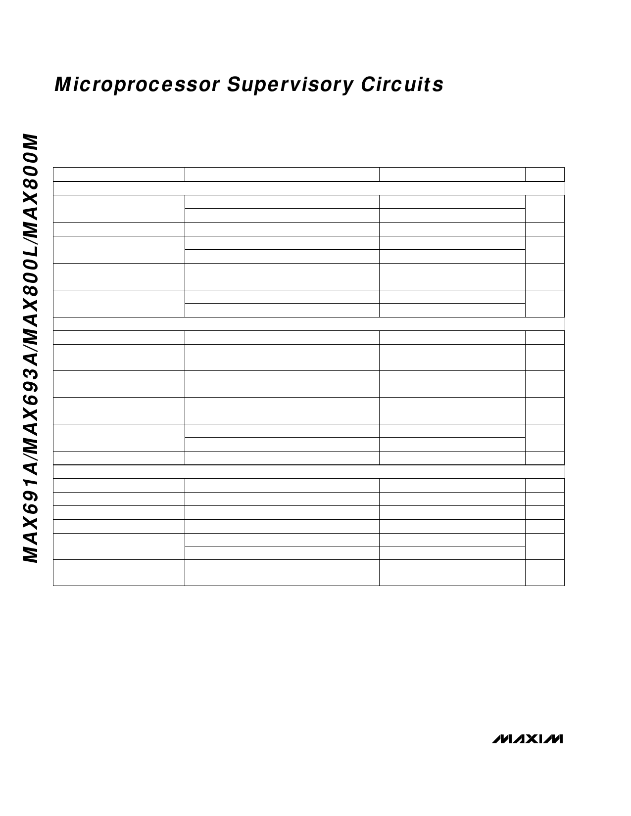
ELECTRICAL CHARACTERISTICS (continued)
(MAX691A, MAX800L: VCC = +4.75V to +5.5V, MAX693A, MAX800M: VCC = +4.5V to +5.5V, VBATT = 2.8V, TA = TMIN to TMAX,
unless otherwise noted.)
PARAMETER
CONDITIONS
MIN
TYP
MAX UNITS
POWER-FAIL COMPARATOR
PFI Input Threshold
PFI Leakage Current
MAX69_AC/AE/AM, VCC = 5V
MAX800_C/E, VCC = 5V
1.2
1.225
1.25
1.25
±0.01
1.3
V
1.275
±25
nA
PFO Output Voltage
PFO Output Short-Circuit
Current
ISINK = 3.2mA
ISOURCE = 1µA, VCC = 5V
Output source current
0.4
V
3.5
1
15
100
µA
PFI-to-PFO Delay
CHIP-ENABLE GATING
CE IN Leakage Current
VIN = -20mV, VOD = 15mV
VIN = 20mV, VOD = 15mV
Disable mode
25
µs
60
±0.005
±1
µA
CE IN-to-CE OUT Resistance
(Note 7)
Enable mode
75
150
Ω
CE OUT Short-Circuit Current
(Reset Active)
Disable mode, –CE OUT = 0V
0.1
0.75
2.0
mA
CE IN-to-CE OUT Propagation
Delay (Note 8)
50Ω source impedance driver, CLOAD = 50pF
6
10
ns
CE OUT Output Voltage High VCC = 5V, IOUT = -100µA
3.5
(Reset Active)
VCC = 0V, VBATT = 2.8V, IOUT = 1µA
2.7
V
RESET-to-CE OUT Delay
Power-down
12
µs
INTERNAL OSCILLATOR
OSC IN Leakage Current
OSC SEL = 0V
0.10
±5
µA
OSC IN Input Pull-Up Current
OSC SEL = VOUT or floating, OSC IN = 0V
OSC SEL Input Pull-Up Current OSC SEL = 0V
10
100
µA
10
100
µA
OSC IN Frequency Range
OSC SEL = 0V
50
kHz
OSC IN External Oscillator
Threshold Voltage
OSC IN Frequency with
External Capacitor
VIH
VIL
OSC SEL = 0V, COSC = 47pF
VOUT - 0.3 VOUT - 0.6
V
3.65
2.00
100
kHz
Note 1:
Note 2:
Note 3:
Note 4:
Note 5:
Note 6:
Note 7:
Note 8:
Either VCC or VBATT can go to 0V, if the other is greater than 2.0V.
The supply current drawn by the MAX691A/MAX800L/MAX800M from the battery excluding IOUT typically goes to 10µA
when (VBATT - 1V) < VCC < VBATT. In most applications, this is a brief period as VCC falls through this region.
“+” = battery-discharging current, “--” = battery-charging current.
Although presented as typical values, the number of clock cycles for the reset and watchdog timeout periods are fixed and
do not vary with process or temperature.
RESET is an open-drain output and sinks current only.
WDI is internally connected to a voltage divider between VOUT and GND. If unconnected, WDI is driven to 1.6V (typ),
disabling the watchdog function.
The chip-enable resistance is tested with VCC = +4.75V for the MAX691A/MAX800L and VCC = +4.5V for the
MAX693A/MAX800M. CE IN = CE OUT = VCC / 2.
The chip-enable propagation delay is measured from the 50% point at CE IN to the 50% point at CE OUT.
4 _______________________________________________________________________________________