MAX2741(2005) Просмотр технического описания (PDF) - Maxim Integrated
Номер в каталоге
Компоненты Описание
производитель
MAX2741 Datasheet PDF : 12 Pages
| |||
Integrated L1-Band GPS Receiver
ABSOLUTE MAXIMUM RATINGS
VCC Pins to GND ...................................................-0.3V to +3.3V
VCC Pins to Each Other .........................................-0.3V to +0.3V
FILT to GND................................................-0.3V to (VCC + 0.3V)
CMOS Inputs to GND (SHDN, SCLK,
CS, SDI).................................................+0.3V to (VCC + 0.3V)
CMOS Outputs to GND (CLKOUT,
GPSIF_, SDO).........................................-0.3V to (VCC + 0.3V)
RFIN to GND...............................................-0.3V to (VCC + 0.3V)
First IF Filter I/O to GND (IFOUT±, IFIN±).....-0.3V to (VCC + 0.3V)
Crystal Inputs to GND (XTAL, REFCLK).....-0.3V to (VCC + 0.3V)
Maximum RF Input Power...................................................0dBm
Continuous Power Dissipation (TA = +85°C)
28-Pin Thin QFN (derate 20.8mW/°C above +70°C) .1000mW
Operating Temperature Range ...........................-40°C to +85°C
Junction Temperature ......................................................+150°C
Storage Temperature Range .............................-65°C to +160°C
Lead Temperature (soldering, 10s) .................................+300°C
Stresses beyond those listed under “Absolute Maximum Ratings” may cause permanent damage to the device. These are stress ratings only, and functional
operation of the device at these or any other conditions beyond those indicated in the operational sections of the specifications is not implied. Exposure to
absolute maximum rating conditions for extended periods may affect device reliability.
CAUTION! ESD SENSITIVE DEVICE
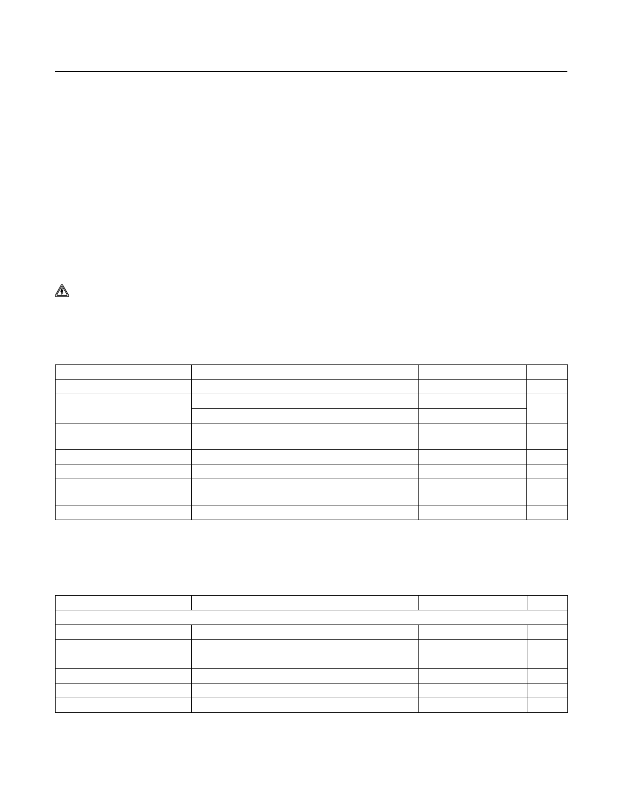
DC ELECTRICAL CHARACTERISTICS
(Operating conditions (unless otherwise specified): VCC = 2.7V to 3.0V; REFCLK driven with 10MHz sinusoid, 1.2VP-P; registers set
according to mode; no RF input signal; digital baseband outputs left open; TA = -40°C to +85°C. Typical values are measured at VCC =
2.75V, TA = +25°C.)
PARAMETER
Supply Voltage
CONDITIONS
MIN TYP MAX UNITS
2.7
3.0
V
Supply Current
Normal operation (TA = +25°C)
Standby (VSHDN = VIL, SYNTH:D8 = 0)
30
42
mA
0.7
Input-Logic High Threshold
VCC -
0.1
V
Input-Logic Low Threshold
Input-Logic High/Low Current
0.1
V
-10
+10
µA
Output-Logic High
ILOAD = 100µA
VCC -
V
0.3
Output-Logic Low
ILOAD = 100µA
0.3
V
AC ELECTRICAL CHARACTERISTICS
(Operating conditions (unless otherwise specified): VCC = 2.7V to 3.0V for TA = -40°C to +85°C; REFCLK driven at 10MHz sinusoid,
1.2VP-P; registers set according to mode; using the Typical Application Circuit; CW RF signal at 1575.42MHz. Typical values are mea-
sured at VCC = 2.75V, TA = +25°C.)
PARAMETER
CONDITIONS
MIN TYP MAX UNITS
1st CONVERSION STAGE (RF TO 1st IF)
RF Frequency
L1-band
1575.42
MHz
RF Conversion Gain
(Note 1)
15
21
32
dB
Noise Figure
Mid-gain (CONFIG1:D4–D0 = 10000)
4.7
dB
Input IP3
(Note 2)
-30
dBm
RF Image Rejection
(Notes 3, 4)
20
35
dB
LO Leakage at RF
LO to RFIN pin
-90
dBm
2 _______________________________________________________________________________________
Share Link: 