HMC5883L Просмотр технического описания (PDF) - Honeywell International
Номер в каталоге
Компоненты Описание
производитель
HMC5883L Datasheet PDF : 18 Pages
| |||
HMC5883L
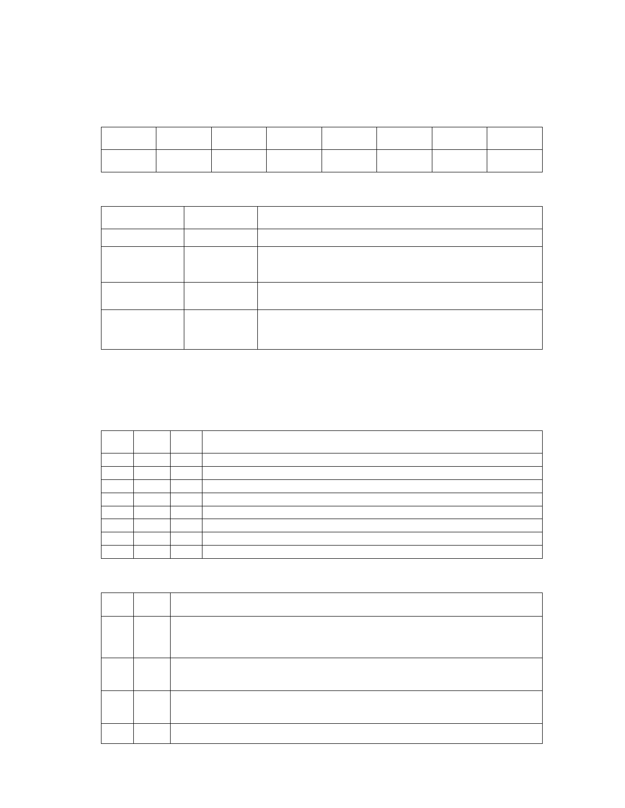
Configuration Register A
The configuration register is used to configure the device for setting the data output rate and measurement configuration.
CRA0 through CRA7 indicate bit locations, with CRA denoting the bits that are in the configuration register. CRA7 denotes
the first bit of the data stream. The number in parenthesis indicates the default value of that bit.
CRA7
(1)
CRA6
MA1(1)
CRA5
CRA4
CRA3
CRA2
MA0(1) DO2 (1) DO1 (0) DO0 (0)
Table 3: Configuration Register A
CRA1
MS1 (0)
CRA0
MS0 (0)
Location
Name
Description
CRA7
CRA7
CRA6 to CRA5 MA1 to MA0
CRA4 to CRA2 DO2 to DO0
CRA1 to CRA0 MS1 to MS0
This bit must be cleared for correct operation.
Select number of samples averaged (1 to 8) per
measurement output.
00 = 1; 01 = 2; 10 = 4; 11 = 8 (Default)
Data Output Rate Bits. These bits set the rate at which data
is written to all three data output registers.
Measurement Configuration Bits. These bits define the
measurement flow of the device, specifically whether or not
to incorporate an applied bias into the measurement.
Table 4: Configuration Register A Bit Designations
The Table below shows all selectable output rates in continuous measurement mode. All three channels shall be
measured within a given output rate. Other output rates with maximum rate of 160 Hz can be achieved by monitoring
DRDY interrupt pin in single measurement mode.
DO2 DO1
0
0
0
0
0
1
0
1
1
0
1
0
1
1
1
1
DO0 Typical Data Output Rate (Hz)
0
0.75
1
1.5
0
3
1
7.5
0
15 (Default)
1
30
0
75
1
Not used
Table 5: Data Output Rates
MS1 MS0 Measurement Mode
0
0
Normal measurement configuration (Default). In normal measurement
configuration the device follows normal measurement flow. The positive and
negative pins of the resistive load are left floating and high impedance.
0
1
Positive bias configuration for X, Y, and Z axes. In this configuration, a positive
current is forced across the resistive load for all three axes.
1
0
Negative bias configuration for X, Y and Z axes. In this configuration, a negative
current is forced across the resistive load for all three axes..
1
1
This configuration is reserved.
Table 6: Measurement Modes
www.honeywell.com
11
Share Link: 