NM25C160TLZET8 Просмотр технического описания (PDF) - Fairchild Semiconductor
Номер в каталоге
Компоненты Описание
производитель
NM25C160TLZET8
Fairchild Semiconductor

NM25C160TLZET8 Datasheet PDF : 10 Pages
| |||
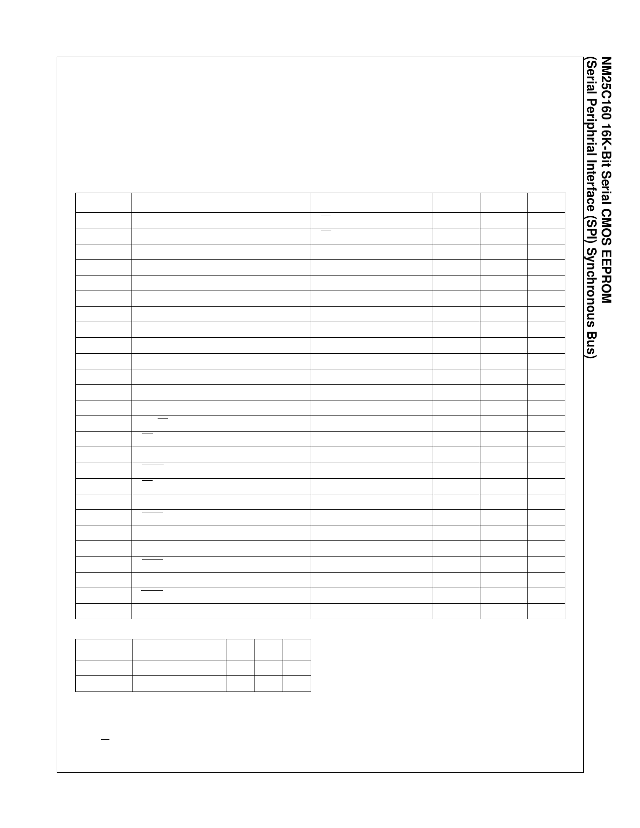
Standard Voltage 4.5 ≤ VCC ≤ 5.5V Specifications
Absolute Maximum Ratings (Note 1)
Operating Conditions
Ambient Storage Temperature
All Input or Output Voltage with
Respect to Ground
Lead Temp. (Soldering, 10 sec.)
ESD Rating
-65°C to +150°C
+6.5V to -0.3V
+300°C
2000V
Ambient Operating Temperature
NM25C160
NM25C160E
NM25C160V
Power Supply (VCC)
0°C to +70°C
-40°C to +85°C
-40°C to +125°C
4.5V to 5.5V
DC and AC Electrical Characteristics 4.5V ≤ VCC ≤ 5.5V (unless otherwise specified)
Symbol
Parameter
Conditions
Min
Max Units
ICC
Operating Current
ICCSB
Standby Current
IIL
Input Leakage
IOL
Output Leakage
VIL
CMOS Input Low Voltage
VIH
CMOS Input High Voltage
VOL
Output Low Voltage
VOH
Output High Voltage
fOP
SCK Frequency
tRI
Input Rise Time
tFI
Input Fall Time
tCLH
Clock High Time
tCLL
Clock Low Time
tCSH
Min CS High Time
tCSS
CS Setup Time
tDIS
Data Setup Time
tHDS
HOLD Setup Time
tCSN
CS Hold Time
tDIN
Data Hold Time
tHDN
HOLD Hold Time
tPD
Output Delay
tDH
Output Hold Time
tLZ
HOLD to Output Low Z
tDF
Output Disable Time
tHZ
HOLD to Output High Z
tWP
Write Cycle Time
Capacitance TA = 25°C, f = 2.1/1 MHz (Note 4)
Symbol
Test
Typ Max Units
COUT
CIN
Output Capacitance
3
8 pF
Input Capacitance
2
6 pF
CS = VIL
CS = VCC
VIN = 0 to VCC
VOUT = GND to VCC
IOL = 1.6 mA
IOH = -0.8 mA
-1
-1
-0.3
0.7 * VCC
VCC - 0.8
(Note 2)
190
(Note 2)
190
(Note 3)
240
240
100
90
240
100
90
CL = 200 pF
0
CL = 200 pF
1–16 Bytes
AC Test Conditions
Output Load
Input Pulse Levels
Timing Measurement Reference Level
3
50
+1
+1
VCC * 0.3
VCC + 0.3
0.4
2.1
2.0
2.0
240
100
240
100
10
mA
µA
µA
µA
V
V
V
V
MHz
µs
µs
ns
ns
ns
ns
ns
ns
ns
ns
ns
ns
ns
ns
ns
ns
ms
CL = 200 pF
0.1 * VCC – 0.9 * VCC
0.3 * VCC - 0.7 * VCC
Note 1: Stress above those listed under “Absolute Maximum Ratings” may cause permanent damage to the device. This is a stress rating only, and functional operation of the
device at these or any other conditions above those indicated in the operational sections of the specification is not implied. Exposure to absolute maximum rating conditions for
extended periods may affect device reliability.
Note 2: The fOP frequency specification specifies a minimum clock period of 1/fOP. Therefore, for every fOP clock cycle, tCLH + tCLL must be equal to or greater than 1/fOP. For
example, if the 2.1MHz period = 476ns and tCLH = 190ns, tCLL must be 286ns.
Note 3: CS must be brought high for a minimum of tCSH between consecutive instruction cycles.
Note 4: This parameter is periodically sampled and not 100% tested.
NM25C160 Rev. D.1
3
www.fairchildsemi.com
Share Link: