BTS728L2 Просмотр технического описания (PDF) - Siemens AG
Номер в каталоге
Компоненты Описание
производитель
BTS728L2 Datasheet PDF : 14 Pages
| |||
BTS 728 L2
Truth Table
Channel 1 Input 1 Output 1 Status 1
Channel 2 Input 2 Output 2 Status 2
Normal
operation
Open load
Overtem-
perature
level
L
H
L
H
L
H
level
L
H
Z
H
L
L
BTS 728L2
H
H
H
L
H
L
L = "Low" Level
H = "High" Level
X = don’t care
Z = high impedance, potential depends on external circuit
Status signal valid after the time delay shown in the timing diagrams
Parallel switching of channel 1 and 2 is easily possible by connecting the inputs and outputs in parallel. The
status outputs ST1 and ST2 have to be configured as a ’Wired OR’ function with a single pull-up resistor.
Terms
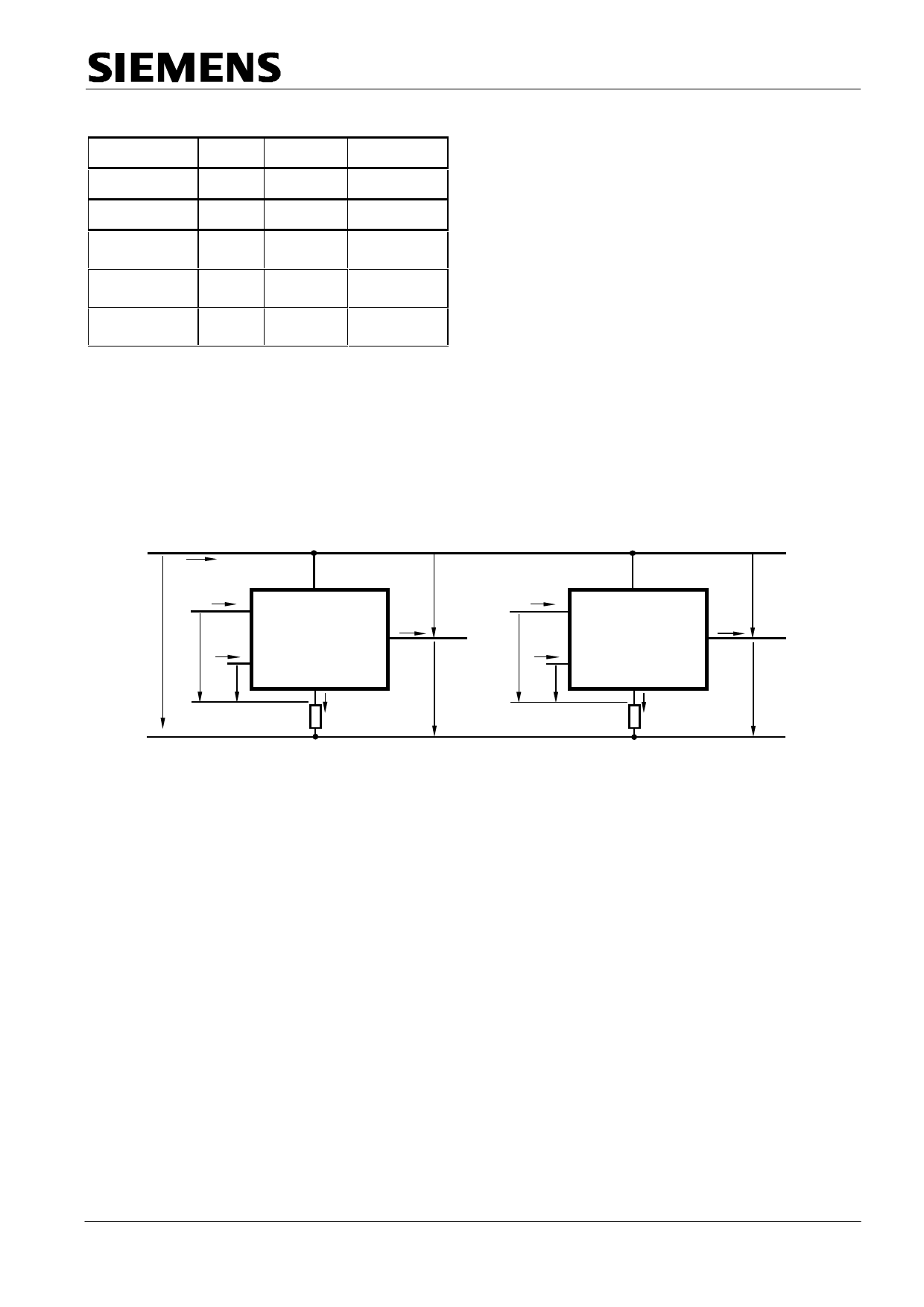
Ibb
V bb
I IN1
IN1
3
Leadframe
Vbb
I L1
I ST1
ST1
4
V IN1 VST1
PROFET
Chip 1
GND1
OUT1
17,18
2
R GND1
IGND1
VON1
V OUT1
V
IN2
I IN2
7
I ST2
8
V ST2
Leadframe
Vbb
IN2
PROFET OUT2
Chip 2
ST2
GND2
6
R GND2
IGND2
I L2
13,14
VON2
V OUT2
Leadframe (Vbb) is connected to pin 1,10,11,12,15,16,19,20
External RGND optional; two resistors RGND1, RGND2 = 150 Ω or a single resistor RGND = 75 Ω for reverse
battery protection up to the max. operating voltage.
Semiconductor Group
Page 7
1999-Mar-23
Share Link: 